Continue to Site

Welcome to EDAboard.com

Welcome to our site! EDAboard.com is an international Electronics Discussion Forum focused on EDA software, circuits, schematics, books, theory, papers, asic, pld, 8051, DSP, Network, RF, Analog Design, PCB, Service Manuals... and a whole lot more! To participate you need to register. Registration is free. Click here to register now.

need help on how to compensate this op-amp

Status
Not open for further replies.

michaelhust

Junior Member level 1
Joined
Sep 30, 2011
Messages
15
Helped
0
Reputation
0
Reaction score
0
Trophy points
1,281
Visit site
Activity points
1,404
Hi, everyone!
For the op-amp compensated in the way as follows, there is a RHP zero a LHP zero lower than the nondominate pole.
That makes it difficult to compensate , so i wonder which position introduces the zeroes and whether there is someway to modify the zeroes to a higher position.
Thanks for your advice!
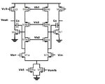
123.JPG
 
Last edited:

At the moment you have compensation loop for bottom portion of first stage only.
Try to create compensation loop for top portion of first stage as well, i.e. to add 2 capacitors between outputs and sources of M3a and M3b accordingly.
Stability will be better.
 
That is indeed a better way to compensate and the op-amp has a better gain margin.
It's very useful . thanks a lot.
 
Last edited:

You're using an Ahuja type of compensation. It's purpose is to eliminate the RHP zero. Interesting why you see RHP zero that's lower than the dominant pole? Putting a capacitor around M3 may help by reducing the loop gain at higher frequencies but it is not addressing the main problem. To a first order the pmos current sources should not affect the stability since they are not in the signal path.
 

I have just tried the method as gevy sad . Though the total value of compensate capacitor are same , the RHP and LHP zeroes indeed move to a higher position with the poles nearly unchanged. So the stability gets better.
As for the problems that you have sad ,I would agree with you before the simulation ,but now I feel really confused.
 
Last edited:

If you feel confused then you'll have to try and understand where the RHP comes from. One place to look is if the M2 transistors are in saturation. Between output of 1st stage and ground you have one Vgs and in this you have to fit 3 Vds of the NMOS stack from the 1st stage.
 

Actually, these are a RHP zero and a LHP zero in the type of Ahuja compensation . Anyone who has the same question could refer to "Issues in “Ahuja” Frequency Compensation Technique ".
With regarding to the improvement as gevy sad, I could not understand yet.
Hope someone could give me some explanations.
Thanks.

---------- Post added at 11:22 ---------- Previous post was at 11:14 ----------

Thanks for your reply. I have carefully arranged 3 Vds to make sure every transistor in saturation.
I have just read a paper about Ahuja compensation named "Issues in “Ahuja” Frequency Compensation Technique".
You can have a look.
 

Yes, I looked at the paper and it indeed shows symmetric LHP and RHP zeros in the frequency response. According to the paper, though, those zeros are at higher frequency compared to the complex non-dominant poles. Also, they are symmetric which means they don't affect the phase response but peak the magnitude response - this, if it happens to your circuit, should not bring problems with stability, if the zeros are after the non-dominant poles. You mentioned that your zeros are before the non-dominant pole, though. There is also one more difference between your circuit and the circuits shown in the paper. Yours is fully differential. The circuits in the paper have a current mirror load for the 1st stage which will affect the dynamics of the amplifier by at least introducing an extra zero coming from the delay of the signal current through that extra path. I'm not sure if the formulas in the paper capture that effect, probably they do. In your case, the load is current sources and is thus not in the signal path. But you still have the effect of the nmos casode transistors through which the Cc current goes. If at frequencies lower than the non-dominant pole the path trough Cc has lower impedance compared to the 1/gm of the cascode devices then you'll have a feed-forward path through the Cc and a RHP zero because of that. Of course I can't know if this is the case with your circuit.
 

Hello, I think after this type of compensation the RHP zero introduced by Cc path is really high.
There must be some other path that introduce the RHP and LHP zeroes.
In my simulation, the symmetric zeroes are before the non-dominant pole and after the unity gain bandwidth.
So they don't influence the phase margin, but they make the gain margin very bad.
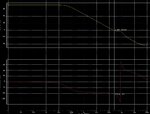
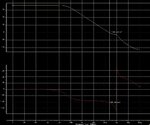
Here you can see the difference between regular Ahuja compensation and the improvement as gevy sad.
The two plots have almost the same unity gain bandwidth,but the second one has better gain margin.regular ahuja compensation.JPGimproved compensation.JPG
 

Actually, it looks to me there is just a single RHP zero there. You first roll-off by -20dB/dec and then it becomes flat, because of the +20dB/dec from the zero. If it were symmetric zeros you'd get peaking because of the +40dB/dec from the two zeros. And this effect is present even in the improved compensation, just shifted. So, whatever is causing it is still there.
 
Last edited:

You'll remember, that insufficient phase margin respectively potential instability of the internal feedback loop has been discussed as cause of the observed frequency characteristic in your previous thread. Did you try anything to confirm or disprove the hypothesis, e.g. analyzing the gain of the internal loop? I also suggested a simple means, placing a series resistor to Cc (not sure, if it helps). Otherwise, a more complex compensation scheme must be implemented for the two stages crossed by Cc.
 

Because these are two poles right after the two zeroes, so it seems these is only one zero. If I modify the zeroes to a lower position, the peaking will be quite obvious.

---------- Post added at 11:11 ---------- Previous post was at 10:50 ----------

Hello, FvM. Nice to hear from you again.
I feel the op-amp that the previous thread mentioned is really complicated for me to analyse the frequency response for time being.
So I select a much simpler version of op-amp and hope to understand the frequency response more clearly.
As long as I am clear about this simple op-amp, I will proceed previous work.
If I have some progress, I will update previous thread and inform you at the same time.
 

Hi,all.
Now I think the overshoot is due to high damping factor of the nondominate complex poles and the zeros have little effect which is different from previous thought.
thanks.
 

Status
Not open for further replies.

Similar threads

Part and Inventory Search

Welcome to EDABoard.com

Sponsor

Back
Top