allennlowaton
Full Member level 5

Hello EDA fellows,
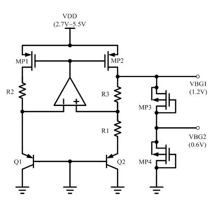
I had used two PMOS that will serve as a voltage divider for the bandgap to produce 1.2V and 0.6V.
I did corner simulations (SS,SF,FS,FF and TT) on the said bandgap and the results went well.
Results for VDD variations (2.7V to 5.5V) and for temperature (-40 to 120deg) are all within an acceptable level.
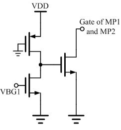
I connect the bandgap to the rest of the circuit and here now comes the problem.
I did a corner on it and the results for SS and FS failed.
TT,SF and FF results are all within an acceptable level.
PMOS device sizes are L=1u , W = 1u and m=4
Below is the simulation results graph.
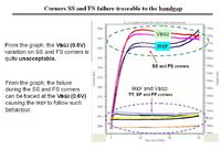
The IREF in the graph is dependent on the VBG2 (0.6V).
I had used two PMOS that will serve as a voltage divider for the bandgap to produce 1.2V and 0.6V.
I did corner simulations (SS,SF,FS,FF and TT) on the said bandgap and the results went well.
Results for VDD variations (2.7V to 5.5V) and for temperature (-40 to 120deg) are all within an acceptable level.
I connect the bandgap to the rest of the circuit and here now comes the problem.
I did a corner on it and the results for SS and FS failed.
TT,SF and FF results are all within an acceptable level.
PMOS device sizes are L=1u , W = 1u and m=4
Below is the simulation results graph.

The IREF in the graph is dependent on the VBG2 (0.6V).

