Continue to Site

Welcome to EDAboard.com

Welcome to our site! EDAboard.com is an international Electronics Discussion Forum focused on EDA software, circuits, schematics, books, theory, papers, asic, pld, 8051, DSP, Network, RF, Analog Design, PCB, Service Manuals... and a whole lot more! To participate you need to register. Registration is free. Click here to register now.

need solution to reduce congestion

Status
Not open for further replies.

chanducs24

Member level 2
Member level 2
Joined
Oct 20, 2010
Messages
53
Helped
0
Reputation
0
Reaction score
0
Trophy points
1,286
Activity points
1,598
hi,

is there any other solution rather than density screens to reduce congestion.

Thanks,
chandra.
 

is it placement congestion or routing congestion. share the detail congestion report.
 

hi

can u tell where i can find that gif?

---------- Post added at 16:53 ---------- Previous post was at 16:31 ----------

hi aravind

it is routing congestion.
 

Try to add the Routing blockage & do the routing. Otherwise, you can alter the cell placement to reduce the routing the congestion.
 
Hi kumar,

your suggestion would be helpful but in which step do i need to add routing blockages? i've tried to add after CTS has been done..i got my routing congestion increased to 30%.. give me some solution.

Thanks,
chandra.
 

Hi Chandra,

Normally routing blockages should be placed before global routing to force global router to respect these blockages. Most Place and Route tools runs the first global routing at placement step and then updates it incrementally, therefore add blockages before placement. Otherwise if you want to use it after any global/detail routing is done, you may need to update global routing first (may be incrementally).

I hope it helps,
Best regards,
Gokhan
---
 

Hi Chandra,
We add placement blockage & routing blockage during the floorplan. Placement blockage is to avoid the unnecessary cell placement in between macros & other critical areas. Routing blockage is used to tell the global router not to route anything on the particular area.Some times people used to change/modify the blockages according to their needs at each stage of the design.
 
Hello

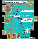
Congestion removal is very simnple..... :)

First analyse placed congested database, and find out the hot spot which is highly congested....

Case -1 "Congestion in Channel between macro"
Reason:- Not enough tracks is available in channels to route macro pins, or channel is highly congested because of std cell placement.
Solution :-Need to increase channel withween Macro or pls. make sure that soft blockage or hard blockage is properly placed.

Case -2:- "Congestion in Macro Corners"
Reason:- Corners of macro is very prone to congestion because its having connectivity from both direction
Solution:- 1. Place some HALo around each macro (5-7um).
2. Place a hard blockage on macro corners (corner protection (Hard Placement Blockage) done after std. cell rail creation otherwise it won't allow std cell inside it"

Case -3 "Congestion in Centre of chip/congestion in module anywhere in chip"
Reason:-Congestion in std. cell or module is based on the module local density (local density is very high 95%-100%)
Also depend on module nature (highly connected)
Die area is less

Solution:- Module density should be even in whole chip (order os 65-85%)
use density screen/Partial blockage to control module density in specific areas.
Use cell pading
if congestion is too big in that case chip area should be increased based on the congestion fig. (it's may be horizontal or Vertical)
congestion_example.JPG
 
Status
Not open for further replies.

Part and Inventory Search

Welcome to EDABoard.com

Sponsor

Back
Top