Continue to Site

Welcome to EDAboard.com

Welcome to our site! EDAboard.com is an international Electronics Discussion Forum focused on EDA software, circuits, schematics, books, theory, papers, asic, pld, 8051, DSP, Network, RF, Analog Design, PCB, Service Manuals... and a whole lot more! To participate you need to register. Registration is free. Click here to register now.

Voltage divisor sensor

Status
Not open for further replies.

sabu31

Advanced Member level 1
Joined
Jan 28, 2011
Messages
467
Helped
12
Reputation
24
Reaction score
13
Trophy points
1,298
Activity points
5,359
Hi

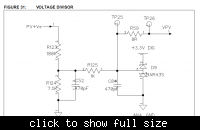
I wanted to design a voltage sensor for giving scaled down voltage input to adc of microcontroller dspic30f2020. I have refered microchip application notes (for dspic33f) and got a circuit (figure 1).

I have two queries. I am not able to understand the use of series resistor R125. Is it just to limit current to adc. Secondly how is the zener diodes functioning in this case as a supply of 3.3V is also given.
Secondly it was mentioned that source impedenced of adc (of dspic30f2020)should be less than 250ohms. So shouldnt R125 be less than 250 ohms.
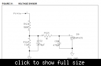
I thought of modifying the circuit as shown. Would this work successfully? Also in the figure1 two grounds were given PV ground and ANalog ground. But should't bothe the grounds be same for sensing the voltage.
[adc can sense maximum of 5V, so zener is around 3.3 or 3.7V)

Thanks
 

I guess R125 is used with C84 for filter. Limit current seems unreasonal because R123 (much bigger) already limits the current.
 
  • Like
Reactions: sabu31

    sabu31

    Points: 2
    Helpful Answer Positive Rating
Input filtering and overvoltage protection has to be designed based on your application requirements. Application notes can at best give an idea or some detail suggestions.

The AN uses schottky diodes for clamping, which allows to limit input voltages without relying on the chip internal clamping diodes. The latter are also specified for +/- 20 mA current handling, but forcing them to forward bias in normal device operation may affect other analog channels. When using zener diodes, you should consider the expectable leakage currents below the nominal zener voltage. In most cases, they'll be inacceptable for an analog input channel.

The source impedance required in the dsPIC datasheet is 1k rather than 250 ohm. Obviously, the idea is to keep errors caused by input currents clearly below 1 LSB. Unfortunately, 1k is not very practical for a high voltage divider. The source impedance of the AN circuit isn't 1k but about 8.2 k, as you may want to calculate. So you'll either accept larger errors (that are hopefully constant and can be calibrated) or you have to place buffer amplifiers.
 

When using zener diodes, you should consider the expectable leakage currents below the nominal zener voltage. In most cases, they'll be inacceptable for an analog input channel.

The source impedance required in the dsPIC datasheet is 1k rather than 250 ohm. Obviously, the idea is to keep errors caused by input currents clearly below 1 LSB. Unfortunately, 1k is not very practical for a high voltage divider. The source impedance of the AN circuit isn't 1k but about 8.2 k, as you may want to calculate. So you'll either accept larger errors (that are hopefully constant and can be calibrated) or you have to place buffer amplifiers.

Hi
Thanks for the reply. However i am not clear about what you meant by "1k is not very practical", is it very less or very high. I am sorry to ask trivial question,but how did u calculate source impedence(any frequency consideration).the source impedence of dspic30f2020 is 100ohms (pg32 adc_2.pdf). Also i came across an article that to reduce source impedence, we connect a high value capacitance at input point of adc channel(adc_source_impedence.pdf). I am not clear about this. They also gave some calculation that C=2047*Cinternal(for 10 bit adc,with error of 1LSB), where Cinternal is the sampling capacitor within microcontroller.However value of Cinternal is not given for dspic30f2020.
So in nutshell, i have to measure 400V dc (approx) using resistor divider consuming 0.25watts, i would have to use 1Mohm and 8.8kohm as resistor divider.ADC sampling frequency is 50Khz.I have to use zener for protection as i dont have low voltage schottky diode.
how do i measure source impedence, and calculate values of required RC filter so that ,impedence observed by the adc input channel is less than 100ohms. also i wouldnt want to use extra opamp circuit. Is it possible.Thanking you.
 

Attachments

  • adc_source_impedence.pdf
    224.7 KB · Views: 69
  • ADC_2.pdf
    511.2 KB · Views: 85

the source impedence of dspic30f2020 is 100ohms (pg32 adc_2.pdf)
1. it's not "the source impedance of dspic30f2020". There's isn't such a thing and it's nothing that can be measured. It's a suggested external impedance to achieve a particular specification.
2. The 100 ohm specification can be found in the dsPIC30F family reference manual. The dsPIC30F3020 datasheet specification is 1k as reported. See TABLE 21-33: 10-BIT HIGH-SPEED A/D MODULE SPECIFICATIONS

However i am not clear about what you meant by "1k is not very practical", is it very less or very high.
Read the next sentence, too. 100 ohm would be in fact less practical.

As the source impedance specification is referring to leakage currents, it's obviously related to a DC source resistance. Capacitors don't play a role in this regard. The DC source "impedance" is the resistance, that's seen when looking from the analog input pin into your circuit. You should be able to calculate it.

Regarding zener diodes as protection devices, I mentioned their leakage currents. You have to determine which zener diodes are suitable for your application. For a 5V analog range, nominal Z diode voltages below 6.8V - 7.5V won't by acceptable in terms of measurement error, I think. So practically, they can only provide a first level protection to keep the current rating of the internal clamp diodes.
 

Hi
Thanks for the info. But there is still some use of external capacitor isnt it. That first attachement adc_source_impedance. was saying that putting an external large capacitor (2047*Cinternal) helps to charge internal cap quickly.Thats why i am confused, because if Cext helps in charging internal cap quickly, it should play some effect in impedance.Got another reference (attachment ADC_1.pdf, pg57).
 

Attachments

  • ADC_1.pdf
    952.6 KB · Views: 69

I didn't yet refer to dynamic behaviour. I wanted to explain Rs related errors caused by the (average) ADC leakage currents, comprised of static leakage and sampling capacitor charge. To avoid additional dynamical errors, you either must assure a sufficient sampling time or provide an additional capacitor to supply the dynamic current during sampling. But Rs is still determing the static measurement error.
 
  • Like
Reactions: sabu31

    sabu31

    Points: 2
    Helpful Answer Positive Rating
Status
Not open for further replies.

Similar threads

Part and Inventory Search

Welcome to EDABoard.com

Sponsor

Back
Top