Continue to Site

Welcome to EDAboard.com

Welcome to our site! EDAboard.com is an international Electronics Discussion Forum focused on EDA software, circuits, schematics, books, theory, papers, asic, pld, 8051, DSP, Network, RF, Analog Design, PCB, Service Manuals... and a whole lot more! To participate you need to register. Registration is free. Click here to register now.

active input regulated cascode current mirror

Status
Not open for further replies.

allennlowaton

Full Member level 5
Full Member level 5
Joined
Oct 5, 2009
Messages
247
Helped
3
Reputation
6
Reaction score
3
Trophy points
1,298
Location
Taiwan
Activity points
3,081
Hello EDA fellows,

I would like to ask some help regarding the
active input regulated cascode current mirror.
Shown below is my circuit.
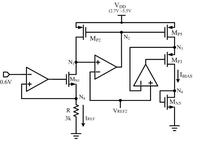

I need to obtain an IBIAS to be a multiple of IREF but
I'm having a difficulty in achieving this.
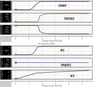
Shown below is my resulted HSPICE simulation.
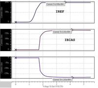

I have observed that I can't make the nodes N1 and N3 to be the same.
I don't understand why.

Thank you for taking time on this.
 

Why so complicated? Why don't you simply adjust the current ratio via the W ratio of transistors? Respectively by an appropriate finger ratio?
 
this circuit will eliminate problems regarding the channel length modulation. Even if the size of the transistor are all the same (l=0.5u, minimum for the 0.35um 5V process), I can't replicate an Ibias that has the same values as the Iref (200uA).
 

Agree with allennlowaton, this structure provides higher current accuracy even when Mp2 and Mp5 stay in linear region.
First, please check if N1 voltage is equal to Vref2. If not, pls debug the first regulation loop. Then check if N3 voltage is equal to Vref2. And debug the second regulation loop.
 
OK, first, check the left OPAMP's input terminal polarities. I guess you might connect uncorrectly or draw the schematic uncorrectly. Second, I guess the other two OPAMPs which are used to clamp the node N1 and N3 to Vref2 level might not be well designed. Try to make sure all of the devices in these two OPAMPs are in active region.

PS: It's not necessary to choose too complex structure for the OPAMPs, a differential pair with mirror load is sufficient. (No complicated frequency compensation)

I hope it would be helpful.
 
Hello EDA fellows,

I would like to ask some help regarding the
active input regulated cascode current mirror.
Shown below is my circuit.


I need to obtain an IBIAS to be a multiple of IREF but
I'm having a difficulty in achieving this.
Shown below is my resulted HSPICE simulation.


I have observed that I can't make the nodes N1 and N3 to be the same.
I don't understand why.

Thank you for taking time on this.

All opamp polarities look correct (negative feedback) so assuming that
- you debugged this successfully with ideal opamps first (because that's the right thing to do)
- and your ideal opamps outputs were clipped to the rails (again a good idea)
my best guess to replicate your problem with real opamps would be that you are chocking the PFET MP5 with too high a voltage on the gate of MP3, because of output range limitations of the 3rd opamp
If you could post the voltage annotated schematic this would be a lot easier

If you are already in trouble with ideal opamps then let us know
 
thank you erikl, leo_02, threekingtiger, dgnani
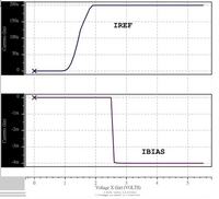
shown below is the simulation result using the Ideal OPs


---------- Post added at 06:08 ---------- Previous post was at 05:55 ----------

Node N1 has the same value (1.2V) as the Vref2, but the node N3 is different.
 

I think vref2=1.2V might be too low. As Ibias increase, Mp3 needs more Vgs.
So I suggest increasing 1.2V to 1.6V, connect Mp3's bulk to its source to remove body effect, and increase Mp3's W/L.
 
hi allennlowaton, is the use of N4 on two separate nodes a typo in the drawing or what you are actually simulating? because in the second case it would be bad
 
I noticed supply is 2.7V for min. So Vref2 could be increased to around 2V. It will help to relax Mp3's W/L.
 
hi allennlowaton, is the use of N4 on two separate nodes a typo in the drawing or what you are actually simulating? because in the second case it would be bad
that node N4 will be used for the other connection of the next stage..
 

I noticed supply is 2.7V for min. So Vref2 could be increased to around 2V. It will help to relax Mp3's W/L.

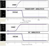
I tried the Vref at 2V, the output looks good but another problem can be seen.
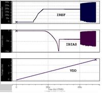
Shown below is the DC and transient analysis:
the DC looks good but the transient looks bad especially at the higher VDD (from 4.4V-5.5V).

TRANSIENT analysis:


DC Analysis:


---------- Post added at 07:47 ---------- Previous post was at 07:46 ----------

yes by why are you using N4 on the first branch as well?

ohh..It's my mistake. A typo. thank you.

---------- Post added at 07:54 ---------- Previous post was at 07:47 ----------

The above simulation results already uses a real op-amp.
No problem can be seen in the transient when the Ideal Op are used.
 

Obviously, transient shows oscillation. So regulation loop needs phase compensation for stability.
 
Ideal OP don't need compensation.
That is the difference.
Pls have AC simulation to design enough phase margin.
DC is correct now.
However, pls check operating point under AC simulation is same as DC sweep.
 
by the way here is another typo for the first opamp the polarities are swapped - I missed that on the first pass, that was the working one after all... you must have it correct in SPICE otherwise it would not work

Congratulations it's getting close
 
Please be aware of that both of loops need stability check. Enough gain will keep good regulation. Enough phase margin keep good stability.
 
Ideal OP don't need compensation.
That is the difference.
Pls have AC simulation to design enough phase margin.
DC is correct now.
However, pls check operating point under AC simulation is same as DC sweep.

thank you leo_o2. I will do what you just said. I learned a lot from you.

---------- Post added at 09:04 ---------- Previous post was at 09:02 ----------

thank you erikl, leo_02, threekingtiger and dgnani..
The EDA won't allow me to click anymore the HELPED button for today.
Tomorrow, I will definitely come back and click them all.
I learned a lot from the masters today.
I will post the results after I did the compensations/adjustments on simulations.
 

Status
Not open for further replies.

Part and Inventory Search

Welcome to EDABoard.com

Sponsor

Back
Top