Continue to Site

Welcome to EDAboard.com

Welcome to our site! EDAboard.com is an international Electronics Discussion Forum focused on EDA software, circuits, schematics, books, theory, papers, asic, pld, 8051, DSP, Network, RF, Analog Design, PCB, Service Manuals... and a whole lot more! To participate you need to register. Registration is free. Click here to register now.

Sine to square 100 MHz converter

Status
Not open for further replies.

zuzu

Member level 3
Member level 3
Joined
Jul 10, 2007
Messages
54
Helped
2
Reputation
4
Reaction score
2
Trophy points
1,288
Activity points
1,817
Hello friends,

Some kind stuck at this stage: sine to square converter (to feed some fpga).
I have a sine wave on 100 MHz with ~3Vrms and need to convert with low jitter to square 3v3.

I tried classic logic buffer with 74F04 (little offset-ed out of 1/2Vdd) 74AC04 (better results, more amplitude) and 74AC14 (best results so far). But the signal out from 74AC14 (all have the same problem) isn't square as it supposed to :)

It's a nice (amplified, clean) sine wave ~4.35Vrms.

Out from last inverter was protected by 47ohm series but no effect, seems not scope capacitance is the problem (I have a Yokogawa 5Gsps @ 500MHz). Maybe propagation delay of buffers is close to limit? But 74AC04 has specified 5nS with 50pF...

Any clues? Or should I just feed FPGA with sine, ac coupled? I am interested in jitter measurements so can (or is even better) to leave sine as is, no more converting?

Any advices greatly appreciated,
 

First try to chop your sine signal then pass it through an integrator ckt.
 

can you be more specific please?
 

zuzu

If you intend to use that square signal to clock, I don´t mind it be a problem.
Note that even clock generated by microcontrollers are not well balanced to half of VDD/GND range ( cicles On and Off are not simetric ).

The most common procedure is to use a high-gain circuit wich saturates output.
A Smith-trigger buffer can perform that.

+++
 

Sounds like a problem of unsuitable signal probing. Although you can't expect a perfect 100 MHz square wave with the said logic families, the output should not look like a sine wave.

Even with perfect signal conditioning, the FPGA contribution to total jitter will be much higher than the jitter of a standard crystal oscillator.
 

Exaclty...in sequencial logic digital systems the wave format don´t matter.
It were syncronized by only one clock edge ( either falling or rising ).

+++
 

Well... the probe is 10 Mohm//20pF.

Yes, plan to clock FPGA, actually to measure (count pulses) of this signal against some other precise time base, inserted also in FPGA as reference. So I thought to low jitter formatting before...
The most common procedure is to use a high-gain circuit wich saturates output.
A Smith-trigger buffer can perform that.
I know, I already tried with 74AC14 but unless amplifying and cleaning effect :) no trace of square at all.. maybe too slow for this 10nS clock ?!

And believe me.. it's a almost perfect sine :) Can you help me improve probing or determine is measuring problem ?
 

I still didn´t realized the problem.

There is common divide oscilator frequency to obtain clock time base.
That division is performed by a single flip-flop.
Thus, it output results in a perfect 50% duty-cycled waveform.

Must be clear that now your timebase will be 20ns ( 50MHz ) and no more 10ns ( 100MHz ).

+++
 

You are appaerntly using a 10:1 passive probe. Has it sufficient bandwidth, e.g. like the Yokogawa 500 MHz probe? Are you using a suitable ground connection? The standard ground probe lead will introduce much inductance and distort the waveform considerably. The short bajonet type ground attachment will give an acceptable ground connection.

For an exact reproduction of a 100 MHz square wave, a resistive low capacitance or an active probe would be needed.
 

Dear FvM,

Exactlly, I used DL9000 series scope (quite expensive, at work) with 500MHz 10:1 passive probe which on Yokogawa web site is rated 500MHz bw, 14pF, 10 MegOhms. Can be ground problems (dead bug style prototype... sorry :)) but that's why I used in the first tests 74F04 which is specified Tp ~3.7nS with 50pF load on 500ohms (I don't use any load, just probe).

Phase signal is little shifted when hands on probe which is normal I presume at this speed. I will try to improve inverter ground connections which now are short (5mm) resistor terminals.

On the other hands, like you pointed earlier, I need this to feed some EPMxx MAX II or some Cyclone (I haven't decided yet). How strong (Vpp) clock needs to be if AC coupled and CPLD input is defined as 1v5 and pre-biased at 1/2? Of course I can do some practically experiments but good to know...
 

As Zuzu mentioned about device could be slower
I think your device should be rated for rise and fall time of less than 1nsec to realize the waveform looks like square.
 

Strictly spoken, tpd hasn't to do with waveforms, only rise- and fall-time matters. But of course, they are partly related, when comparing logic families.

I still think, that the said sine waveforms are a case of unsuitable probing. As already said, you need very short ground connection (directly to the "coaxial" tip connector) with standard passive probes. If you are frequently facing similar measurement problems, you should think about a low capacitance active or passive resistive probe. Even a 10:1 or 20:1 divider formed by a chip resistor and a 50 ohm coax cable connected to the 50 ohm oscilloscope input can be a reasonable alternative.

Also insufficient supply bypassing of the logic gate can be a reason to get bad waveform.

Regarding FPGA interface, I would prefer a differential I/O standard if you can't assure sufficient voltage swing. I have also used external LVDS receivers as level converter. As they are not generally specified for this mode of operation, you have to check the empirical behaviour. Logic thresholds of single ended FPGA standards aren't tightly specified, so you have to provide sufficient input level, on the other hand, the maximum voltage range should be kept safely. Just as an idea, how about a self biased FPGA input circuit using an inverted output and a high ohmic resistor?
 

I agree with FvM. 74AC parts have about 20 ohm output R at 3.3V so should be giving 1 nS rise/fall times.
 

Ok, thanks all very much for valuable comments.
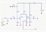
I decided to re-design a bit speaking to my colleagues.. Since I need this signal inside FPGA only (and is coming from ext. analog multiplier) I will try to multiply inside, bu using embedded PLL. So sine to square is no more need. Anyhow, I simulate a bit some schematic proposed by Sir Charles Wenzel in one of his excellent articles with good results @ 100 MHz and I post here if anyone needs. For levels under 0.5Vpp output is kept sine, but over 0.7Vpp and up tp 2Vpp a nice limiting effect appears, the signal is square and depending on R9 (and or R3) value, can be tuned for FPGA I/O bank level (I choose here 1V5). Sim is a MonteCarlo 9 levels.
 

Attachments

  • sinetosquare.gif
    sinetosquare.gif
    69.3 KB · Views: 281
  • sinetosquare2.gif
    sinetosquare2.gif
    27.9 KB · Views: 265
Status
Not open for further replies.

Part and Inventory Search

Welcome to EDABoard.com

Sponsor

Back
Top