allsey87
Member level 4

Hey All,
I have a design which consists of two PCBs stacked on top of each other interconnected by a 100mil header on each side of the board.

The main source of power is applied to the bottom PCB where there are switching regulators to step down the voltage.
The design has been completely captured inside a single altium project, where as a top level schematic file contains the headers and two schematic sheet objects which represent both the top and bottom layers of the design (see page 5 of View attachment swarmEBv2.pdf)
To route the power between the bottom and top PCBs, and into the schematics further down the hierarchy, I was using power ports connected to schematic ports, however this generates a warning during compile, that I have reduced the global power port object to local scope, I didn't realise this until I got that message, but it does make sense.
So now I'm removing all the power ports and replacing them with schematic ports in the design, but this causes warning about ports having the same name. so now I'm considering using a single port to represent the power in and out of each module (shematic), and distributing the power inside that schematic using simple net labels, which I know have local scope only.
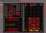
As a quick sanity check, the reason why I'm avoiding using the global power ports is that I don't want Altium complaining about me not making routes between the two PCBs which have been arranged side by side during routing (see image below).

So I guess my question is, how is one suppose to go about this sort of project? what experiences have you had? how can one change the scope of a power port object? or solve this problem in a nice clean and logical way - I think I know of a **** (why is the word h-a-c-k not allowed?) to get this working, but still, it would be nice to know the 'correct/the altium way'...
I have a design which consists of two PCBs stacked on top of each other interconnected by a 100mil header on each side of the board.

The main source of power is applied to the bottom PCB where there are switching regulators to step down the voltage.
The design has been completely captured inside a single altium project, where as a top level schematic file contains the headers and two schematic sheet objects which represent both the top and bottom layers of the design (see page 5 of View attachment swarmEBv2.pdf)
To route the power between the bottom and top PCBs, and into the schematics further down the hierarchy, I was using power ports connected to schematic ports, however this generates a warning during compile, that I have reduced the global power port object to local scope, I didn't realise this until I got that message, but it does make sense.
So now I'm removing all the power ports and replacing them with schematic ports in the design, but this causes warning about ports having the same name. so now I'm considering using a single port to represent the power in and out of each module (shematic), and distributing the power inside that schematic using simple net labels, which I know have local scope only.
As a quick sanity check, the reason why I'm avoiding using the global power ports is that I don't want Altium complaining about me not making routes between the two PCBs which have been arranged side by side during routing (see image below).

So I guess my question is, how is one suppose to go about this sort of project? what experiences have you had? how can one change the scope of a power port object? or solve this problem in a nice clean and logical way - I think I know of a **** (why is the word h-a-c-k not allowed?) to get this working, but still, it would be nice to know the 'correct/the altium way'...
