Continue to Site

Welcome to EDAboard.com

Welcome to our site! EDAboard.com is an international Electronics Discussion Forum focused on EDA software, circuits, schematics, books, theory, papers, asic, pld, 8051, DSP, Network, RF, Analog Design, PCB, Service Manuals... and a whole lot more! To participate you need to register. Registration is free. Click here to register now.

About free license band rf module (315Mhz & 433Mhz)

Status
Not open for further replies.

sysysy

Member level 3
Member level 3
Joined
Nov 11, 2010
Messages
56
Helped
2
Reputation
4
Reaction score
1
Trophy points
1,288
Activity points
1,801
Hello,

I am doing a project and trying hard to understand the operation theory of this type of RF module(315Mhz and 433Mhz).

From the datasheet, it say that the RF transmitter just will transmit out the data whenever there 'see' the data at the data pin....Hmmm, in my project, of course i put the data that i want to that pin through the microcontroller.

But the problem raise up in my mind, how actually this rf module work?
Are the transmitter juz simply modulate the data to 315hMhz with the data and send out and the receiver do the demodulation for the data?

For a asynchronous communication, both side of my microcontroller must need to have a same baud rate. let say i set both in 4.8k baud rate... so, how this baud rate affect my rf module? becoz from the module, i see the receiver have its own crystal mean clock...but transmitter does not have... i suspect they also need have their own baud rate in communication instead of we set it in microcontroller... how to relate this?

i really feeling blur to this...juz hope anyone can explain and lead me to correct track. Thanks alot.
 
Last edited:

Basically the RF output is 433MHz is wat they mean
 

To show you how your module work, you should give some info about them.

From what you're saying it seems that these modules use OOK modulation. The transmitter need an accurate frequency set, it can be through a SAW filter if you haven't seen any XTAL on board.

My guess is that you are right: you can see the TX as a simple data modulator to 315 MHz and RX as a simple demodulator.

Please upload a spec, so I can help you more in detail.

Mazz
 

Most of the OOK modules are nothing more than a single transistor oscillator with the data input providing bias to the transistor. A '0' at the input stops the oscillator and a '1' starts it. The crystal or resonator is there just to maintain the frequency. The receiver for these is just detects the presence of a carrier and reports it as a '1' for present and '0' for absent.

Some modules have built in processors and encode the data to increase reliability, for example using Manchester encoding. In that kind of module your data is sent to the processor so the Baud rate has to match what the processor expects. These modules usually use FSK rather than amplitude keying.

You need to look at the data sheet to decide which is best suited for your needs, they both work of course but have their own advantages and disadvantages.

Brian.
 

    V

    Points: 2
    Helpful Answer Positive Rating
Hi, thanks for the reply...

Actually i do not have the exact datasheet since i bought in somewhere electronics shop. I juz refer to the internet standard datasheet since they are doing the same thing.

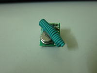
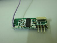
Anyway, i do capture down the snapshot of both of the tx and rx RF module.


There is no crystal in the transmitter side but do have a (HLC 4.897) crystal in the receiver side... the modulation method maybe in ASK or OOK? But juz really very interested how is this module operating theory since i am not in telecommunication field student. i search some info about OOK and ASK.

Although my main task just use in as a wireless communication tool in my project, but reallly interested with this whole module. Honestly, it is very hard to find a details description for this type of module or circuit.

To be more clear, i listed down few question below, juz hope anyone who have knowledge in this field can share about this.

1. In OOK technique, is it to see whether the digital data ('1' or '0' ) presence or absence of a carrier? OK, let say now the carrier signal is in 315Mhz. so how this data encapsulate inside with this carrier?

2. In the RF transmitter, just consider there must a 315mhz modulator on the circuit (i suspect is this component is like a coin shape silver cap?)for modulate purpose. But then, where is the part decide what modulation technique that use? ASK or OOK?

3. Then how the data transmit out? without follow the clock? since there is no crystal in Tx side but do have a crystal in receiver side? and the CS3411 chip (high speed viterbi decoder) in rx side...in the progress understanding the datasheet about it now.... :oops::oops::oops:

4. So in RF receiver side, once the receiver detect the 315Mhz signal, it juz will automatically demodulate it and retrieve the signal? how it regconize noise around? or impossible the existence of 315Mhz noise around?

5. last question, is it RF module is never related with UART? is juz a communication tool... but why this tool have a bit rate or baud rate limit?

Notes: I'm sorry if some question already redundant with the answer that you guys already answer. Anyway, really feel great if anyone willing to share share the knowledge or provide me some material.

ALso, i attached the similar module datasheet (315Mhz and 433Mhz)
https://www.cytron.com.my/datasheet/WirelessDevice/RF_TX_User's_Manual.pdf
 

    V

    Points: 2
    Helpful Answer Positive Rating
1. 0 = no carrier at all, 1 = carrier being transmited.
2. The silver can is a SAW resonator to set the frequency, there will be a single transistor on the board as well. The data input pin will be connected to the transistors bias circuit so 0/1 turns the oscillator off/on.
3. I doubt the IC is a Viterbi decoder, it is more likely to be a PLL oscillator and homodyne receiver. 64 x crystal frequency is just below 315 MHz.
4. Basically, what comes out is a signal strength reading which should follow the level received by keying the transmitter on and off. Noise will probably cause spurious output so filtering and verifying data in software is a good idea.
5. The data rate limit is cause by the time it takes for the oscillator to start up and shut down at the transmitter and the time it takes for the receiver to react the the incoming signal strength change.

Brian.
 
  • Like
Reactions: sysysy

    sysysy

    Points: 2
    Helpful Answer Positive Rating
    V

    Points: 2
    Helpful Answer Positive Rating
Hi betwixt,

I really appreciate for your explanation. Thank a lot.

Hmmm, i have a very silly question here :oops:
0 = no carrier at all, 1 = carrier being transmited.
I interpret it that no carrier is mean there is no 315Mhz frequency transmitted out, then when there is 1, carrier being transmitted out.

So that's mean in a byte of data RF module transmit out will have 2 frequency which is 315Mhz (represent '1') and 0Hz (represent '0'). Am i right?

Ok, then again let say we have a byte of data which is '11010010' to transmit out... so, the wave shuold look like in pattern
315Mhz 315Mhz 0hz 315Mhz 0hz 0hz 315Mhz 0Mhz

Then finally i wanna conclude that, that mean the transmitter will not only send out only 315MHz signal out since it is also have 0hz stuff inside? But other frequency will be 100% be filtered?

I doubt the IC is a Viterbi decoder, it is more likely to be a PLL oscillator and homodyne receiver. 64 x crystal frequency is just below 315 MHz.

i will said that it use viterbi decoder is because there is a chip CS3411 in a receiver side. and i google it online and found that the datasheet saying it is a high speed viterbi chip. But anyway, there is another XTAL (HLC 4.897) in a receiver side, maybe this is a clock for the viterbi chip(doubting) since the chip do have a clk pin.

betwixt,
i'm also feel sorry for asking so much, i should go do more research actually.
but it is really too much mathematical expression in those modulation technique part and also the viterbi algorithm that very hard to be understand directly.

regards,
sysysy
 

sysysy

forget about viterbi decoding. The part number you found there has nothing to do with it. Most probably is the MICRF002YM, same band, same supply, package and same pinout (from what I'm able to unserstand in you photo), same XTAL. You can start studying this doc for a better understanding.

You are right about the way TX OOK works (Ok, then again let say we have a byte of data which is '11010010' to transmit out... so, the wave shuold look like in pattern
315Mhz 315Mhz 0hz 315Mhz 0hz 0hz 315Mhz 0Mhz).

OOK means ON OFF KEYING. The 0Hz case you mention is simply the 'OFF' state. The data input pin simply control the on/off state of an oscillator tuned at 315MHz, so when you send '1' you simply turn on the oscillator, sending '0' you turn it off (do a test measuring current consumption in the two cases, if you want to check).

I hope it can help.

Mazz
 
  • Like
Reactions: sysysy

    sysysy

    Points: 2
    Helpful Answer Positive Rating
    V

    Points: 2
    Helpful Answer Positive Rating
100% agree with Mazz !

It doesn't transmit 0Hz, it transmits nothing at all when the data input is zero. The data pin is actually nothing more than an on/off control for the oscillator. When '0', nothing comes out, when '1' the 315MHz comes out.
Other than a maximum speed at which the oscillator can start up there is nothing limiting the speed of the data. If you send standard serial data all you get is pulses of 315MHz corresponding to the 1's and 0's in the data.

The complicated end is the receiver, it has to pick up the signal and give you an output telling you if 315MHz was seen or not. It isn't as easy as it sounds because in the absence of signal it will pick up background noise and maybe other devices using the same frequency nearby. To help identify a 'real' signal the receiver usually filters out very short bursts of 315MHz and only tells you when it has found something it *thinks* is real data, bear in mind that different receivers will do this in different ways and some don't do it at all. The receivers data output is essentially a signal strength indicator so if all is well, it follows the pattern of the signal from the transmitter as the carrier appears and disappears.

Most receivers use some kind of automatic gain control (AGC) to help them cope with both strong and weak signals, it is usually recommended you send a long '1', maybe for half a second or more before the data itself, this gives the receiver chance to adjust its gain so there is less chance of it missing the first few bits of the data.

Forget Viterbi completely - it is an error correcting mechanism used on high speed digital links and far, far, far more advanced than this simple link requires.

Brian.
 

    V

    Points: 2
    Helpful Answer Positive Rating
Hi,

Thanks for the reply, i do digest something from both of you explanation. thank you so much...

Anyway, since i have something doubt,

Mazz say
You are right about the way TX OOK works (Ok, then again let say we have a byte of data which is '11010010' to transmit out... so, the wave shuold look like in pattern
315Mhz 315Mhz 0hz 315Mhz 0hz 0hz 315Mhz 0Mhz).

But Brian say
It doesn't transmit 0Hz, it transmits nothing at all when the data input is zero.

so transmit nothing is not equal to 0hz????

Then Brian say again
The complicated end is the receiver, it has to pick up the signal and give you an output telling you if 315MHz was seen or not.

But since only data '1' will be in 315Mhz signal and data 0 is ntg (even not a 0Hz), that mean the receiver only can interpret 315Mhz as data '1'. So how the receiver interpret the so-called data 0?( ntg or 0hz)???

Ok, then back to transmitter side,
as Mazz say, a byte data '11010010', we can represent it as wave in form (315Mhz 315Mhz 0hz 315Mhz 0hz 0hz 315Mhz 0hz)... but how they remain in air in this form? i quite confuse with this? receiver really can interpret that it is a byte of sequence data, especially the data '0'.
 

0Hz is not a frequency ! It is the absence of frequency !

When the data pin at the transmitter is held at logic '1' the transmitter sends out a 315MHz carrier. It keeps transmitting the carrier until the data pin is taken to zero again.
When the data pin at the transmitter is held at logic '0' the transmitter is shut off, nothing comes out of it at all.

The data output from the receiver is '1' when it hears a carrier and stays at '1' until the carrier can no longer be heard. When it can't hear any carrier it's data output is '0'.

Nothing 'remains' in the air, for all practical purposes the signal leaving the transmitter arrives at the receiver instantaneously. To send a byte of data, the transmitter sends it one bit at a time and the receiver picks it up one bit at a time. It is up to the circuitry at the transmitter to break the byte into individual bits and send them at a particular speed. The circuit after the receiver has to work at the same speed and reconstruct the bits into the byte again. Do a search on 'UART', it will explain the process of shifting bytes out as bits and reconstructing them again later.

Brian.
 
Status
Not open for further replies.

Part and Inventory Search

Welcome to EDABoard.com

Sponsor

Back
Top