Continue to Site

Welcome to EDAboard.com

Welcome to our site! EDAboard.com is an international Electronics Discussion Forum focused on EDA software, circuits, schematics, books, theory, papers, asic, pld, 8051, DSP, Network, RF, Analog Design, PCB, Service Manuals... and a whole lot more! To participate you need to register. Registration is free. Click here to register now.

Basic question on capacitotrs in Spectre

Status
Not open for further replies.
500MSPS is high sample rate and you probably can use time interleaved DAC architecture to give ur charge redistribution dac more time to settle. what specs are u targeting for ?
 

I'm bothered only about speed of DAC .can u please give me some good papers on interleaved DAC architectures.
When I searched on net for DAC architectures I have found that some of them are having DNL and INL about 3to 4LSB.Won't there be any problem using that DAC in an ADC?
 

Hi all,
I've used bottom plate sampling technique in this circuit.

Even using this circuit I'm getting signal dependent glitch in my output.I don't know how to add dummy switch for this bootstrap switch.If any one have some ideas plz share with me.
one more basic question is if I increase rise time(also fall time) of control signal by two times why doesn't amplitude of glitch reduce by 2 times?
 
Last edited:

... if I increase rise time (also fall time) of control signal by two times why doesn't amplitude of glitch reduce by 2 times?
Because the glitch amplitude depends on the C-ratio. The C values don't change by changing the slew rate.
 

but to me it seems like is something similar to that of inverter where the overlap capacitance couples some amount of input to output.And to decrease glitch we increase slew rate of signal at gate.Here also peak of the glitch doesn't reduce to half if we increase slew by two times.
 

In an inverter, there is always a low impedance path to conduct any such coupled charges (ie either by the NMOS or PMOS or both), so any transient coupling will be less obvious when slew rates are reduced.
Here, there is no low impedance path. Any coupled charges will simply stay there, be it a fast coupling or slow coupling, until it slowly leaks away into the substrate.
That is why the capacitance value in switched cap is always bounded on the lower end by
1. Matching
2. Parasitics
 
@checkmate:Even with bottom plate sampling I'm getting signal dependent glitch!!how to over come this issue.
And even size of dummy transistor is effecting amount of glitch by few tens of volts.Should the size of the dummy transistor be always half the size of main switch always?

---------- Post added at 16:59 ---------- Previous post was at 16:54 ----------

In the circuit shown below will the GBW of opamp determines the maximum sampling rate DAC?

34_1297855676.png
 

@checkmate:Even with bottom plate sampling I'm getting signal dependent glitch!!how to over come this issue.
And even size of dummy transistor is effecting amount of glitch by few tens of volts.Should the size of the dummy transistor be always half the size of main switch always?
Bottom plate sampling only forces all (or at least the majority) of charge injection towards the same node of the switch, which can be later cancelled off via differential circuits. It does not reduce any "glitches". Furthermore, it does not handle the other non-idealities.

Dummy switches reduces clock feedthrough, but the degree of reduction is totally non-reliable. The half-sizing rule makes the assumption that both ends of the switch sees the same impedance, and therefore any feedthrough charges are distributed equally on both ends. Realistically speaking, how possible is that?

Lastly, if you are still using 5fF caps, your only option is to either reduce parasitics, or increase your cap.

In the circuit shown below will the GBW of opamp determines the maximum sampling rate DAC?
34_1297855676.png
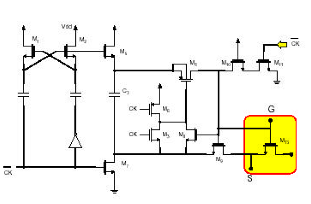
The maximum sampling rate is largely determined by the settling time of the opamp.
 
Lastly, if you are still using 5fF caps, your only option is to either reduce parasitics, or increase your cap

I've changed my capacitance to 20fF but bootstrap switch isn't tracking input signal.And if size of bootstrapped transistor is increased so as to drive the capacitor it is resulting in larger glitches at capacitor top plate.
 
Last edited:

increasing ur bootstrapped transistor size increases ur parasitic caps, so this will cause a good deal of charge redistribution with your sampling cap. if your sampling cap is high compared to the parasitic cap then the effect will be less. if u are taping out the design then size ur cap based on matching/parasitics rather than noise.

I've changed my capacitance to 20fF but bootstrap switch isn't tracking input signal
- your switch isnt designed properly...
 

I've changed my capacitance to 20fF but bootstrap switch isn't tracking input signal.And if size of bootstrapped transistor is increased so as to drive the capacitor it is resulting in larger glitches at capacitor top plate.
Then have you considered that you are targeting a sampling rate that is so high that it is not achievable by your process?
 

34_1297855676.png

@checkmate:If I use this ciruit I will get differential output(vout+,vout-) but I think I can connect only one of its terminals to capacitor.So how can I manage with these outputs? Do I need to use Differential to single ended OTA??

Can I use this cicuit..?
44_1298023095.png

Please reply to my Posts....
 
Last edited:

Adding dummy transistor helps to reduce charge injection and clock feed-thru. As the result, the glitch will be suppressed.

I've changed my capacitance to 20fF but bootstrap switch isn't tracking input signal.And if size of bootstrapped transistor is increased so as to drive the capacitor it is resulting in larger glitches at capacitor top plate.
 

Adding dummy transistor helps to reduce charge injection and clock feed-thru. As the result, the glitch will be suppressed.
But dummy transistor should be fed with inverted control signal,then how can I generate inverted signal as the bootstrap switch is controlled by some complex circuitary....

---------- Post added at 15:56 ---------- Previous post was at 14:48 ----------

Bottom plate sampling only forces all (or at least the majority) of charge injection towards the same node of the switch, which can be later cancelled off via differential circuits. It does not reduce any "glitches". Furthermore, it does not handle the other non-idealities.
@checkmate:In document you have suggested it is said that we will have only fixed charge injection and fixed feed thru,but I'm getting signal dependent charge injection.
 

That's because you have totally disregarded that your problem has a parasitic component which I suspect is a major factor with a 5fF cap, and not only charge injection and clock feedthrough. You should really try to evaluate alternate architectures, or try some sort of interleaved architecture to lower your sampling rate.
 

What value of capacitance you think is appropriate?
one more question is if it results in only fixed charge injection and fixed clock feedthrough can't we think of its as only offset error and remove it using a level shifter rather using a differential opamp?
You should really try to evaluate alternate architectures, or try some sort of interleaved architecture to lower your sampling rate.
Does interleaved architecture mean using two parallel ADCs?
 

1. you can use the amplifier circuit shown in our post as long as it provides u required gain and bandwidth
2. try out some switch (basic transmission gate & bootstapped) with different cap values (5f , 20f, 100f , 200f) -- u will find the glitch to reduce as u increase the cap. dummy are useful in reducing clock feed thru and to some extent charge injection. bootstrapped will require voltages which will go above you normal vdd - so reliability will be an issue.
3. interleaved ADC mean parallel ADCs architecure. (ex) u can have 2 ADCs working at 250msps and mux there inputs and outputs.
4. u will always have a some sampling error at inputs as long as this error is not signal dependent then u can consider them to be offset (dc errors) if u use differential structure the error is assumed to be same and will get rejected by the opamp due to its CMRR.
 
Thanks all,
I have changed capacitor to 10pf ,now charge injection is below 20mV.But my sample and hold circuit is taking around 600ps to track input voltage,can anybody suggest me some high speed sample and hold circuits that don't have opamps in them.
 

Status
Not open for further replies.

Part and Inventory Search

Welcome to EDABoard.com

Sponsor

Back
Top