Continue to Site

Welcome to EDAboard.com

Welcome to our site! EDAboard.com is an international Electronics Discussion Forum focused on EDA software, circuits, schematics, books, theory, papers, asic, pld, 8051, DSP, Network, RF, Analog Design, PCB, Service Manuals... and a whole lot more! To participate you need to register. Registration is free. Click here to register now.

MOSFETs with built in reverse current diodes

Status
Not open for further replies.

stube40

Member level 3
Member level 3
Joined
Feb 10, 2010
Messages
55
Helped
4
Reputation
8
Reaction score
4
Trophy points
1,288
Location
Queensland, Australia
Activity points
1,825
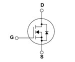
Alot of MOSFETs come with a built-in diode across the source and drain. The attached diagram outlines what I mean. I would like to confirm that the purpose of this diode is to allow the MOSFET to handle reverse current to flow.

I know this question might sound really dumb, but I'm not an electronics expert.

Further, if this is indeed the case, is it possible to exploit this diode to enable the MOSFET to allow reverse current in an application where we expect regular reverse currents?

Finally, which particular parameters in the data sheet for a MOSFET describe the diode's maximum reverse current and how long it can maintain this current for?
 

Attachments

  • MOSFET Outline.JPG
    MOSFET Outline.JPG
    27.3 KB · Views: 198

Alot of MOSFETs come with a built-in diode across the source and drain. The attached diagram outlines what I mean. I would like to confirm that the purpose of this diode is to allow the MOSFET to handle reverse current to flow.

No, it's to indicate source is internally connected to body of MOSFET.

Body is the substrate where source,drain reside (refer structure of a MOSFET); Sorce,drain are formed with same type of semiconductor and body is in opposite type of them.

Since body forms diodes with source & drain, this connection means "diode between drain and source".

Further, if this is indeed the case, is it possible to exploit this diode to enable the MOSFET to allow reverse current in an application where we expect regular reverse currents?

No, this diode means we can only use MOSFET for one direction; not for bidirectional signals.

Finally, which particular parameters in the data sheet for a MOSFET describe the diode's maximum reverse current and how long it can maintain this current for?

Couldn't find such "diode's maximum reverse current". But this source-body connection affects to drain-source breakdown voltage, which is mentioned in datasheets.

Thank you,
 

OK, thanks for your quick reply.

Maybe I could fit a real diode externally across the source and drain - do you think this would work?
 

I see at least some misunderstandings suggested by the previous answer.

The circuit symbol shows both, substrate connection of the source (the arrow in the centre of the MOSFET) and a diode between source an drain. As stube40 mentioned, the diode between source and drain is actually a side effect of the source-substrate connection, it's also called body-diode. The schematic symbol doesn't particularly suggest to utilize the body diode in your circuit design, it simply tells about it's existence.

Many power MOSFET datasheets have however a detailed specification of the body diode. It's current rating is useally similar to the active drain current, in some cases even higher, see e.g. IRF540. The body diode has mostly standard recovery time, except for some special designed MOSFET, and this may be a reason to connect an external schottky diode in parallel. Connecting an external p-n diode is almost useless, because the body diode will conduct anyway and cause slow recovery.

There are many circuits that make use of the body diode, e.g. bridge inverters.
 
Hi,
What is your application ?
Is it controlling bipolarity signal (current is not significant ) or control power supply (larger current) ?

Thank you
 

Hi FvM,

Thank you for such descriptive clarification.

I missed to explain distinguishing "the arrow in the centre of the MOSFET" is the connection to substrate-source and effect of this connection is the body-diode.

Could you please comment my answer to "exploit this diode to enable the MOSFET to allow reverse current in an application where we expect regular reverse currents";
Isn't it no ?, I mean existence of this body-diode will not make MOSFET to use for bidirectional signal controlling. (eg. work as a switch for bipolarity signal)

And, couldn't find this "diode's maximum reverse current" in datasheets;
I guessed stube40 need some idea about drain-source characteristics; so mentioned about "drain-source breakdown voltage" which has some effect of this body-diode.

Thank you and highly appreciate your comments.
 

My understanding is, that the original poster don't want to use the MOSFET to handle bipolar voltages higher than the forward voltage of the body diode, which won't work of course. Also reverse current doesn't mean reverse current of the diode rather than forward current.
 
Thanks for all the helpful replies.

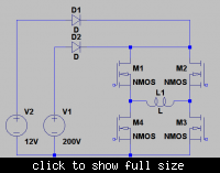
My application is that I'm using 2x MOSFETs to select between two LA batteries as the supply to system which charges/discharges a superconducting coil via a 4x MOSFET H-bridge. I've attached a diagram which shows what I mean (note, all MOSFETs are IXYS IXFK230N20T N-channel enhancement mode).

Note, the H-bridge system is already built and works fine (we super-cool the MOSFETs using liquid nitrogen and they become rock-solid).

The idea is that one of the LA batteries is 2V and the other is a battery bank running at 200V - kind of psuedo 'fast' and 'trickle' charges. The coil has an inductance of approx 50mH.

We charge to 40A and have chosen MOSFETs that can handle this with adequate cooling. Depending on the scenario and the external magnetic field applied to the coil, sometimes we a reverse current at the battery terminals and it is my fear that this will kill the 2x new MOSFETs switches I'm proposing to select between 12V and 200V battery supply.

I was wondering whether fitting an adequately spec'd diode across source and drain of S1 and S2 would protect against this.


If you follow the current path through you will see that the S2 Body Source diode is always biased on feeding the 200V source to the bridge and its load. It looks like you are expecting to 'slowly' charge up your 'superconductor' to some current level and then switch it off at some 'controlled' rate of dI/dT.... or voltage... or it does not.

What are you really trying to do and how fast do you wish to go??

Genome.

Edit

Oh, as others have mentioned the Body-Source diode is an intrinsic parasitic that results from the way the device is constructed. 'Generally' you will find it has the same average current ratings and peak current ratings as the device itself.

https://www.vishay.com/docs/91070/91070.pdf

Drain Current,


Diode Current,


There is a steady state thermal limit, wire bonding limit and a transient thermal impedance limit.

As suggested they are the same but your mileage may vary since for different devices the diode forward drop may result in different levels of dissipation.

Apart from it being a diode and having the associated characteristics if you are dealing with transient conditions then you have to refer to the transient thermal impedance curves,


Just to 'make sure' things do not audibly go 'dink'.

Then again I'm sure those curves 'do not apply' at -197C

8O
 
Last edited:

Hi Genome,

The idea is to use the 200V supply to rapidly charge the coil to 40A in 10ms: (50mH * 40A) / 200V == 10ms. This is equivilant to a rate of 4000A per s.

After we reach 40A we use the two bottom MOSFETs in the H-bridge to short-circuit the coil. The current in the coil will dissipate slowly due to losses in the MOSFETs and the contacts. We can top it up gradually by switching to the 2V LA battery and charging at a much lower rate of 40A per s. This results in lower AC losses overall in the coil that charging using the 200V supply.

I hope that all makes sense.

I didn't quite follow what you meant by "If you follow the current path through you will see that the S2 Body Source diode is always biased on feeding the 200V source to the bridge and its load".
 
OK... think it does but it's late.

Regarding selection of the sources and your proposed circuit.. If I take out the Mosfets and just leave their body-source diodes in then the circuit becomes,


Effectively D2 puts the top of the bridge at 200V and D1 is reverse biased so the lower voltage never gets a 'look in'.

As I say the explanation makes sense, sort of. However it's late over here and I have just scoffed food so it's time for bed.

Later

Genome.
 

Source and body / "neck" are always tied in a power MOSFET / DMOS
structure. However this tie is not always stout enough for high current
or so low resistance you would want to use it that way. And the lifetime
is liable to be high especially in high voltage (high resistivity) FETs. If
your current reverses (FET goes back to right-side-up) while the body
is still full of carriers, say hello to Mr. Parasitic BJT and smell the sweet
smell of "buy another FET". And maybe some other stuff too.
 

As far as I understood, you're mixing two objectives of your circuit, battery reversal protection and battery selection.

It has been already pointed out, that the circuit can't work this way. This hasn't to do with the particular properties of the MOSFET body diode and can't be healed by connecting anything in parallel. It's just a case of not considering what the circuit does.

To have reversal protection and the battery switch option, you need a bidirectional switch at least for the 200 V battery, better for both to allow power down of the circuit without disconnecting the 12 V battery. A bidirectional switch can be formed by two "anti-serial" connected FETs, preferably source-to-source, which is a usual configuration for AC/DC capable solid state relays.

When using an active switch as battery-reversal protection, which is effectively required to achieve a low voltage drop, then you have to care of course for correct control of the gate voltage. Otherwise the protection will be void.

As an off topic guess, it sounds like you are a physicist?
 
Hi Genome,

The idea is to use the 200V supply to rapidly charge the coil to 40A in 10ms: (50mH * 40A) / 200V == 10ms. This is equivilant to a rate of 4000A per s.

After we reach 40A we use the two bottom MOSFETs in the H-bridge to short-circuit the coil. The current in the coil will dissipate slowly due to losses in the MOSFETs and the contacts. We can top it up gradually by switching to the 2V LA battery and charging at a much lower rate of 40A per s. This results in lower AC losses overall in the coil that charging using the 200V supply.

I hope that all makes sense.

I didn't quite follow what you meant by "If you follow the current path through you will see that the S2 Body Source diode is always biased on feeding the 200V source to the bridge and its load".

Hi Stube40

I think I've got the gist of it. Some questions.

Do you need to reverse current in the coil or is it just the case that you want to get it up to a specific level of current and then maintain it there over time?

Is the rapid charge a strict requirement?

You mention AC losses. Can you explain more about those?

This is a picture of a simple Synchronous Buck converter,


Inductor set via M1 free wheels, or resets, through M2. The mosfets are driven in anti-phase with duty cycle setting the output voltage. In simpler converters M2 would just be a diode and, as you can see, the body source diode of M2 would behave as such. They 'are' generally rated to do this, as long as it says so on the data sheet, but as others have mentioned the characteristics of the diode unless the device is processed correctly is nothing to write home about.

In the case of synchronous rectification when free-wheeling current is flowing through the diode the Mosfet is switched on, the drain channel is resistive and current can and does flow through it in both directions. With the Mosfet on then the majority of the current flows in the Drain with a resulting lower voltage drop and reduced power losses in the circuit.

Of course.... if you do this,


Then things might begin to look 'familiar'.

It is a 'perfectly acceptable' thing to do as long as you apply 'current mode control' to the power switches and with correct sensing you would be able to set the current quite precisely. The question would be do you mind 'high frequency' voltage excursions at one end of your coil and the associated 'ripple current' in it?

Keeping things simple then there is a 'soft' limit to how high VIN can be. Basically you can get level shifted drivers rated up to 100V that would do the job quite nicely. You can go higher but then control of things like cross-conduction becomes more of an issue.

Do Hall Effect Current Probes work down to the temperatures you are using or do they 'magically' lose their properties as well?

Genome.
 

As an off topic guess, it sounds like you are a physicist?

Hi FvM,

I'm not a physicist, but good guess. 1st degree in Electronic Engineering, PhD in Robotics (google "Robug IV"). Industry experience in many areas, most of which involve embedded systems of somesort. About 70% of expertise lies in programming, 30% in electronics. All low-power 3.3V / 5V stuff. Power Electronics is something I've got no experience in.

Is the attached diagram what you had in mind? If so, should I use individual isolated gate controllers? Finally, do you turn them both on at the same time when you want +VE current to flow to the system then turn them both off to isolate the battery?

**broken link removed**

---------- Post added at 00:24 ---------- Previous post was at 00:02 ----------

Hi Genome,

Yes, we need to reverse the current in the coil. Ideally we are trying to put a square wave through it at +/- 40A. Since it takes a finite time to charge the inductor from -40A to +40A (20ms @ 200V), the square wave is actually trapezoidal.

Yes, rapid charge is important to get as close to square as possible.

AC losses is an area of superconductors not very well understood as yet. Basically, if you put a DC signal into a superconductor in perfect conditions then there are no losses what so ever and you get perfect power transfer. If you put an AC signal into the same superconductor in the same perfect conditions then there will be losses involved, most of which result in the superconductor heating up causing accelerated losses as the superconductor moves away from it's working temperature. The loses are proportional to the rate of change of amplitude. Hence, our target square wave described above is the worst case scenario and exhibits more losses than a sine wave. Once the coil reaches 40A, there are less AC losses if you use a smaller voltage to top it up since the change in amplitude is slower. In summary, the nature of our system leaves us with no choice other than to charge to 40A as fast as we can, resulting in high AC losses. However, we try to offset this by minimising the AC losses involved in maintaining the 40A "steady-state" stage of the square wave.

We currently use a hall-effect sensor (Allegro ACS758) to detect the current in the H-bridge and we use a micro to perform the overall control. Hall effect probes dont work past -40deg or so, but we keep them separate from the cold stuff.

Whilst your email on the Sync Buck was really helpful and informative, I couldn't quite work out how this relates to making the battery-selection switching part work. As I mentioned earlier, I'm a total noob with regards to power electronics and only have limited experience at normal electronics, so my appologies if I'm appearing fairly stupid.................
 

I confess, the physicist guess was brought up as you reported, you're cooling MOSFETs with LN2... But it's not meant depreciative, just a specific way to look on things. I personally started to study physics before changing to engineering, and the fundamentals are still helpful.

The bidirectional MOSFET switch is correct this way. Please notice, that for on-off control, both gates can be connected to a common isolated circuit, driving a voltage between the gates and the common source nodes. As mentioned, you can buy AC/DC solid state relays, that either have a DC/DC converter or a simple (slow switching) photovoltaic optocoupler to isolate the control signal.

Regarding AC behaviour of superconductors, isn't it so, that infinite conductance implies zero penetration of AC current thus infinite current density? How is this point treated in SC theory?
 
Thanks FvM,

Cooling the MOSFETs with liquid nitrogen was just a short-cut - it meant that we didn't have to invent a way of cooling it using conventional methods, it also meant we could use a MOSFET with RdsOn of 7.5mOhm well outside of it's SOA. A small tip to anyone listening - that 7.5mOhm turns into something that is a tiny fraction of that at -77K. We have been amazed at the hyper-efficiency of some MOSFETs at this low temperature.

AC losses - we've proven that we get losses using AC signals that we dont get with DC signals. We can estimate the losses by measuring the additional boil-off rate of the liquid nitrogen through the additional heat energy generated by the coil due to the AC losses. We have models that describe why this happens at a molecular level, but it would take someone more knowledgeable than me to explain it to you.

OK, so finally I understand the orientation of the bidirectional MOSFET switch although I must admit to not fully understanding why it can handle both forward and reverse current. Referring back to my picture earlier in this thread, can I simply replace S1 with a bidirectional MOSFET switch? Similarly, replace S2 with a second bidirectional MOSFET switch? Will this finally be the solution that enables me to control whether the 12V battery or 200V battery is supplying the H-bridge?
 
OK, thanks.

The synchronous buck would not solve your battery selection problem and I was 'hoping' that the AC problem wasn't there. OK, I was pushing my luck. As suggested the synchronous buck would have given you very precise control of the current from 0 up to your 40A and would have maintained the 'holding' current to similar levels. Instead of switching batteries you would just let the feedback deal with things and used a single high voltage source. Given AC is a real issue, I sort of did not doubt it but.... then it looks like that was and is a no go. On top of that you also want the bi-directional drive and, in a similar way, your full-bridge might have done the same.. but AC is a problem so that won't work as well.

You say you do not know power electronics.. I don't know low temperature Physics. That might make us quits..;-)

I should bite my tongue but I tried to visualise things and I can almost see why this will not work. No, it must be the frequency that matters. I was kind of thinking that narrower pulse widths even at higher voltages to maintain the same 'regulation' would result in the same integrated ripple and so.... Head implodes. There may be something in what I am thinking but on the other hand I'm not so sure.

Looks like FvM has your solution so I won't butt in on their reply to your latest questions.

Genome.
 

I must admit to not fully understanding why it can handle both forward and reverse current.
I assume, you fully undestood, why a single FET can't handle it. Because the diode enables current in one direction without a means to stop it. Now, in off-state, the current flow will be blocked by one of the FETs having a positive Vds. The other will conduct above 0.5 to 0.7 V. In on-state a MOSFET will have it's low rdson for both current polarities. The switch resistance is however doubled, because both MOSFET's rdson is summed.

Will this finally be the solution that enables me to control whether the 12V battery or 200V battery is supplying the H-bridge?
Yes. But you have to care to interlock both battery switches, otherwise theres a danger to short the batteries.
 

Status
Not open for further replies.

Similar threads

Part and Inventory Search

Welcome to EDABoard.com

Sponsor

Back
Top