Continue to Site

Welcome to EDAboard.com

Welcome to our site! EDAboard.com is an international Electronics Discussion Forum focused on EDA software, circuits, schematics, books, theory, papers, asic, pld, 8051, DSP, Network, RF, Analog Design, PCB, Service Manuals... and a whole lot more! To participate you need to register. Registration is free. Click here to register now.

Silvaco Software code or script

Status
Not open for further replies.

shoofeer1

Newbie level 5
Newbie level 5
Joined
Jul 4, 2009
Messages
10
Helped
5
Reputation
10
Reaction score
5
Trophy points
1,283
Activity points
1,422
Hi all,

I am doing a project that needs me to design a PMOS transistor with a channel length of 65 nanometers using Silvaco TCAD tools. As you may know, there are examples provided in the software that I am using to customize in order to get the required channel length. So, I have to modify the silvaco Code to get what I want. But the problem is there is no much reference material and it is like shooting in the dark. Could any one help me and let me know which specific part of the code do I need to change? Please help and I will be forever grateful.
 

This is a very quick rough 65nm PMOS with comments. Let me know if you need any further explanations:

go athena
#
#To allow changing device size, set the gate length as a variable
set Lg=0.065
#
#Set up a mesh suitable for a 65nm MOSFET. The MOSFET will be symmetrical
#so just model half of the device starting mid channel at 0.0.
#Only need to model out to 0.1um so final transistor will be placed in the middle
#of a 0.2um mesh in x direction
line x loc=0 spac=0.01
line x loc=0.5*$Lg spac=0.005
line x loc=0.1 spac=0.1
#
line y loc=0.00 spac=0.005
line y loc=0.3 spac=0.015
line y loc=0.5 spac=0.02
line y loc=2 spac=1
#
# Start off by defining silicon as p type <100> with boron conc=2e15
init orientation=100 c.boron=2e15

#Deposit an oxide on the silicon surface for implanting to prevent channeling
deposit oxide thick=0.05

#nwell formation for the body of the pmos transistor. The shallowest implant
#will define the threshold voltage so vary to get desired threshold.
implant phos dose=2.6E13 energy=420 tilt=5
implant phos dose=3.5E13 energy=50 tilt=5

#Anneal the nwell and electrically activate it
diffus temp=1000 time=100 weto2 hcl=3

#Remove all oxide prior to gate oxidation
etch oxide all

#Grow a thin gate oxide target 2.5nm. Change steps 2,3,4 to adjust thickness
#
method fermi compress
diffuse temp=700 time=34 f.o2=0.5 f.n2=10 t.final=800 pres=1
diffuse temp=800 time=2 f.o2=20 pres=1
diffuse temp=800 time=3 f.o2=10 f.hcl=0.1 pres=1
diffuse temp=800 time=2 f.o2=10 pres=1
diffuse temp=800 time=10 inert
diffuse temp=800 time=20 inert t.final=700
#Display actual gate thickness acheived
extract name="Thin Gate Tox" thickness oxide mat.occno=1 x.val=0

#Deposit 200nm Gate Poly.
deposit poly thick=0.2 division=20

#Dope the poly P-Type
implant boron dose=5.0e15 energy=15 tilt=5

#Etch the poly gate
etch poly right p1.x= 0.5*$lg

#Deposit Spacer TEOS and etch to form the oxide spacer
deposit oxide thick=0.02 division=8
etch oxide thick=0.02
struct outf=exspacer.str

#P+ Source Drain Implant (PSD). This is a very shallow implant for 65nm
#which is why we had to dope the poly earlier.
implant boron dose=1.0e15 energy=4 tilt=0

#Anneal PSD using spike (very fast) RTA
diffusion temp=1000 time=2 seconds f.o2=0.3 f.n2=2.7
struct outfile=expsdrta.str

#Now need to form silicide on the Source Drain and Gate regions.
#130nm and below uses sputtered Cobalt to form CoSi.

#First remove all oxide from surfaces where CoSi is to be formed.
etch oxide thick=0.014

#Sputter 40nm Cobalt
deposit cobalt thick=0.04 div=8

#Use RTA to react Cobalt with Silicon to form CoSi
diffusion temp=550 time=10 second inert

#Strip away any unreacted cobalt from non silicon surfaces
#e.g. the spacer oxide.
etch cobalt all
struct outfile=exsal.str

#mirror the structure to form the complete transistor
structure mirror left
struct outfile=final.str

#Define the electrodes
electrode name=drain x=-0.08
electrode name=source x= 0.08
electrode name=gate x= 0
electrode name=substrate backside
#-----------------------------------------------------------------------------
go devedit
base.mesh height=1000000 width=1000000
bound.cond !apply max.slope=28 max.ratio=300 rnd.unit=0.001 line.straightening=1 align.points when=automatic
imp.refine imp="NetDoping" sensitivity=1
imp.refine min.spacing=0.01
constr.mesh max.angle=90 max.ratio=300 max.height=1 max.width=1 min.height=0.0001 min.width=0.0001
Mesh Mode=MeshBuild
refine mode=both x1=-0.5*$Lg y1=0 x2=0.5*$Lg y2=0.2
############# PVt Test : Returns PVt, PBeta and PTheta ################
go atlas
# set material models
models cvt srh print
contact name=gate p.poly
interface qf=3e10

# get initial solution
solve init


method newton trap
solve prev

# Bias the drain a bit...
solve vdrain=-0.1 name=drain

# Ramp the gate
log outf=mos1ex08_1.log master
solve vgate=0 vstep=-0.05 vfinal=-1.5 vdrain=-0.1 name=gate
save outf=mos1ex08_1.str

quit
 
Thank you so much for the kind help Colbhaidh, I am really grateful.
Please allow me to ask the following:

Q1. According to ITRS (International Technology Roadmap for Semiconductors), we cannot just reduce the gate length (by the way, when we say for e.g a 65 nm p-MOS, do we mean the gate is 65 nm or is it the channel length) but we should also scale other parameters such as:

1. Threshold voltage
2. Gate oxide thickness
3. Junction depth
4. Junction depth at the source
5. Junction depth at the drain
6. contact Junction depth
7. Channel dopant concentration.....and some other parameters.

Hence, which parts of the code govern the above said parameters ?

Q2. In the part of the code that says:
"#nwell formation for the body of the pmos transistor. The shallowest implant
#will define the threshold voltage so vary to get desired threshold.
implant phos dose=2.6E13 energy=420 tilt=5
implant phos dose=3.5E13 energy=50 tilt=5"
why do we have two statements? in the original example given in Silvaco, there is only one statement. Also, what does "shallowest implant" mean ?

Q2. Is the part of the code that says:
#Etch the poly gate
etch poly right p1.x= 0.5*$lg
the statement that determines the gate length solely? are there other statements that control this too?


I apologize if I asked too many questions and I hope that you will be able to lend me a hand with this as your kind help is much appreciated.
 
OK First thing: the only stupid question in the universe is the one that was never asked!

For a 65nm process, this generally refers to the physical gate length of the poly, so the actual channle length is much lower (~40nm).
Having said that, many Semiconductor companies claim to have a 65 nm process that is actually a 90nm physical gate length with a 65nm electrical gate length. Fortunatley, this is rare.

Threshold voltage is an adjustable parameter. Since Idsat is determined by threshold voltage, you want the lowest threshold voltage. However Off state leakage is also determined by threshold voltage so you want the highest threshold voltage. So Threshold voltage is a compromise. The body effect of two mos transistor is series (say for an AND gate) also means the threshold voltage has to be such that a circuit will work, so 500mV-700mV is typical to allow logic gates to be reliably formed. But if your Vdd is 1.2V and threshold is 600mV then your overhead is pretty badly reduced.
Gate oxide thickness is also a parameter for threshold voltage so physics determines that it must be thin for 65nm. Howevber if it is too thin it will conduct current (and self destruct as a consequence) so again their is a compromise. This is controlled by the Gate Oxide diffuse statements in the code above.
Junction depth itself is not the problem, but the deeper the junction, the more lateral diffusion of the junction and the effective gate length decreases to the point the transistor is shorted. So junction depth is the maximum possible without that lateral diffusion that causes the effective gate length to be unusable. For 65nm this is very shallow. This is controlled by the implant dose and energy in the P+ implant statements ain the code. Just change the implant energy in the TCAD to see the effect of deeper junctions!
Channel doping determines the threshold voltage but also contributes to the off state leakage and breakdown between drain and source. This is why 65nm and smaller uses lower voltages. A 65nm transistor would be shoirted at 3.3V but operates well at 1.2V.
Now the breakdown between source and drain you want this to happen below the surface of the channel (deep in the bulk) for reliability reasons. To do this you can change the doping of the NWell with depth by using 2 or more implants. The higher the energy of the implant the deeper it will go so9 in the code there are two implants: one with higher energy for the deep part of the NWell the other lower energy to determine the surface channel doping and hence the threshold voltage. In a real process, I would probably use 3 implants.
Silvaco examples are very simple and rarely reflect the real world.
Gate physical length is controlled by etching the gate poly so this does determine the gate length alone. But the electrical gate length is controlled by the lateral diffusion of the P+ implanbt under the gate poly.
 
Thanks once more for the VERY elaborate and detailed help. I'm now very comfortable with gate length modification. I've tried modifying the following

1. Gate oxide thickness
2. Threshold voltage

for the gate oxide thickness, I tried to scale it down from (0.00371855 A°to 0.001A°, which is given by ITRS table) but the values stagnated at 0.002A°. I've changed all the Tox statements in the code. What could be the problem?

The threshold voltage also seems to be randomly fluctuating when I modify the Vth Adjust implant statement. Mathematically,
Vth = Vto +γ( √(Vsb + 2Φ)- √2Φ)
and,
γ= (Tox/εox)√(2qεNa).....

Hence, shouldn't the Thickness Tox, be affecting the Threshold voltage?
I am also getting a positive value for Vth, which I guess should be -ve since I am dealing with PMOS.

The code doesn't include "extract parameter"...So I included the following statements which I took from Silvaco example codes:


# Extract other design parameters...
# extract final S/D Xj...
extract name="pxj" xj silicon mat.occno=1 x.val=0.1 junc.occno=1
# extract the long chan Vt...
extract name="p1dvt" 1dvt ptype vb=0.0 qss=1e10 x.val=0.49
# extract a curve of conductance versus bias....
extract start material="Polysilicon" mat.occno=1 bias=0.0 bias.step=0.2 bias.stop=2 x.val=0.45
extract done name="sheet cond v bias" curve(bias,1dn.conduct material="Silicon" mat.occno=1 region.occno=1) outfile="extract.dat"
# extract the P++ regions sheet resistance...
extract name="p++ sheet rho" sheet.res material="Silicon" mat.occno=1 x.val=0.05 region.occno=1
# extract the sheet rho under the spacer, of the LDD region...
extract name="pldd sheet rho" sheet.res material="Silicon" mat.occno=1 x.val=0.3 region.occno=1
# extract the surface conc under the channel....
extract name="pchan surf conc" surf.conc impurity="Net Doping" material="Silicon" mat.occno=1 x.val=0.45

Hence, how should I change these statement too, especially the values that are in bold/red ?

I heard about other things like Halo doping and well-drive, what are they? are they necessary?

Other than these parameters (threshold voltage, gate length, Oxide thickness, Junction depth, channel doping concentration...) what else should be done such that the design is optimum? is deciding these parameters the end of the story?

I thank you again once more for the kind help, and look forward to your enlightening response...
 
Dear Colbhaidh,

is there any process flow for 180nm?

thanks
 

A gate oxide thickness of 0.00371855 A° is much less than the diameter of 1 atom so this is very wrong.
a 65nm process has a gate thickness of about 1.8nm or more (18A°).

The following gives a 15nm gate oxide with a VT of ~0.18V

go athena
#
#To allow changing device size, set the gate length as a variable
set Lg=0.065
#
#Set up a mesh suitable for a 65nm MOSFET. The MOSFET will be symmetrical
#so just model half of the device starting mid channel at 0.0.
#Only need to model out to 0.1um so final transistor will be placed in the middle
#of a 0.2um mesh in x direction
line x loc=0 spac=0.01
line x loc=0.5*$Lg spac=0.005
line x loc=0.1 spac=0.1
#
line y loc=0.00 spac=0.005
line y loc=0.3 spac=0.015
line y loc=0.5 spac=0.02
line y loc=2 spac=1
#
# Start off by defining silicon as p type <100> with boron conc=2e15
init orientation=100 c.boron=2e15

#Deposit an oxide on the silicon surface for implanting to prevent channeling
deposit oxide thick=0.05

#nwell formation for the body of the pmos transistor. The shallowest implant
#will define the threshold voltage so vary to get desired threshold.
implant phos dose=2.6E13 energy=420 tilt=5
implant phos dose=1.0E13 energy=50 tilt=5

#Anneal the nwell and electrically activate it
diffus temp=900 time=100 weto2 hcl=3

#Remove all oxide prior to gate oxidation
etch oxide all

#Grow a thin gate oxide target 1.5nm
#Uses rapid thermal oxidation (simplified)
method fermi compress
oxide init=0.0001
diffuse temp=1000 seconds time=26 dryo2
#Display actual gate thickness acheived
extract name="Thin Gate Tox" thickness oxide mat.occno=1 x.val=0

#Deposit 200nm Gate Poly.
deposit poly thick=0.2 division=20

#Dope the poly P-Type
implant boron dose=1.0e15 energy=15 tilt=5

#Etch the poly gate
etch poly right p1.x= 0.5*$lg

#Deposit Spacer TEOS and etch to form the oxide spacer
deposit oxide thick=0.02 division=8
etch oxide thick=0.02
struct outf=exspacer.str

#P+ Source Drain Implant (PSD). This is a very shallow implant for 65nm
#which is why we had to dope the poly earlier.
implant boron dose=1.0e15 energy=3 tilt=0

#Anneal PSD using spike (very fast) RTA
diffusion temp=1000 time=2 seconds f.o2=0.3 f.n2=2.7
struct outfile=expsdrta.str

#Now need to form silicide on the Source Drain and Gate regions.
#130nm and below uses sputtered Cobalt to form CoSi.

#First remove all oxide from surfaces where CoSi is to be formed.
etch oxide thick=0.014

#Sputter 40nm Cobalt
deposit cobalt thick=0.04 div=8

#Use RTA to react Cobalt with Silicon to form CoSi
diffusion temp=550 time=10 second inert

#Strip away any unreacted cobalt from non silicon surfaces
#e.g. the spacer oxide.
etch cobalt all
struct outfile=exsal.str

#mirror the structure to form the complete transistor
structure mirror left
struct outfile=final.str

#Define the electrodes
electrode name=drain x=-0.08
electrode name=source x= 0.08
electrode name=gate x= 0
electrode name=substrate backside
#-----------------------------------------------------------------------------
go devedit
base.mesh height=1000000 width=1000000
bound.cond !apply max.slope=28 max.ratio=300 rnd.unit=0.001 line.straightening=1 align.points when=automatic
imp.refine imp="NetDoping" sensitivity=1
imp.refine min.spacing=0.01
constr.mesh max.angle=90 max.ratio=300 max.height=1 max.width=1 min.height=0.0001 min.width=0.0001
Mesh Mode=MeshBuild
refine mode=both x1=-0.5*$Lg y1=0 x2=0.5*$Lg y2=0.2
############# PVt Test : Returns PVt, PBeta and PTheta ################
go atlas
# set material models
models cvt srh print
contact name=gate p.poly
interface qf=3e10

# get initial solution
solve init


method newton trap
solve prev

# Bias the drain a bit...
solve vdrain=-0.05 name=drain

# Ramp the gate
log outf=mos1ex08_1.log master
solve vgate=0 vstep=-0.05 vfinal=-1.0 vdrain=-0.1 name=gate
save outf=mos1ex08_1.str

quit

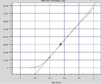
Note that when I calculate VTH, I use the way a Fab would do it. That is take the max slope of Vgs vs Ids, find the maximum (max dIds/dVds) and calculate the intercept with Vgs axis and subtract 0.5*Vds.
For this example I used a Vds of 0.5V. The intercept was 0.21V giving a VTH of 0.185.

For slight adjustments, adjust the energy of the well implant
implant phos dose=1.0E13 energy=50 tilt=5


A halo implant is used to compensate the channel beneath the gate where reducing L brings the source and drain implants beneath the channel causing VTH to drop. So the halo implant is a 45 degree implant either side of the poly to knock out the P+ of the SD beneath the channel.


What specific 0.18um process are you looking for.
 
Dear colbhaid

Thanks a ton! I hope you had very happy holidays :)

Here is a code for 100 nm process (it is based on Silvaco examples 9 and 8), it seems that everything is ok but the threshold voltage seems to be very large. Also, when I use two extract statements for Tox (1 right after gate oxide growth and another right before other extract statements), the first one stays invariably the same no matter what value(s) I alter, while the second one varies slightly. BTW, I use the results produced in results.final file for all parameters (Vth, Tox, junction depth...etc) Hence, results.final says the following:


Code:
gateox=20 angstroms (0.002 um)  X.val=0.005------------>first Tox result

gateox=17.7442 angstroms (0.00177442 um)  X.val=0.005---->second one
p1dvt=2.6415e+14 V  X.val=0.49-----------------> very strange value of Vth


For this process, a Vth of 0.2 V, a gate oxide of 1.5-2 nm, and junction depth of 40 - 80 nm are required. Could you please lend a hand in getting these values ? (at least the first two, while keeping the Vgs vs Ids curve the same)

btw, you seem to not use extract statements. How do you find Tox and Vth?
 
is Devedit the one that produced the graph you provided (and calculated the max slope) ?

Thanks again and I am looking forward to your kind help. Here is the code: 

--------------------------------------------------------------------------
# This is a simple input deck representing a Process flow and a device
# test. All lines beggining with a '#' sigh may be treated as directive
# comments..... 
# Start the Athena Process simulator running...
go athena
#
# Set up a mesh suitable for a single MOSFET device....
line x loc=0 spac=0.1 
line x loc=0.35 spac=0.02
line x loc=0.5 spac=0.1
#
line y loc=0.00 spac=0.005 
line y loc=0.3 spac=0.015
line y loc=0.5 spac=0.02
line y loc=2 spac=0.2 
line y loc=5 spac=1 
#
# Start off by defining silicon with 1e14 phos doping...
# Decrease the folowing space.mult parameter for a denser
# mesh and more accuracy...
init orientation=100 c.phos=1e15 space.mult=2
#
#pwell formation including masking off of the nwell
#
diffus time=30 temp=1000 dryo2 press=1.00 hcl=3
#
etch oxide thick=0.02
#
#N-well Implant
implant amorphous phos dose=1.0e12 energy=100 pears
#
diffus temp=950 time=100 weto2 hcl=3
#
#N-well implant amorphous not shown -
#
# welldrive
diffus time=220 temp=1200 nitro press=1
#
etch oxide all
#
#sacrificial "cleaning" oxide
diffus time=20 temp=1000 dryo2 press=1 hcl=3
#
etch oxide all
#
#gate oxide grown here:-
set partial_press=1.0
diffus time=9  temp=350 nitrogen hcl=1
diffus time=2  temp=450 dryo2 press=$partial_press
diffus time=11 temp=422 dryo2 press=$partial_press hcl=1
diffus time=8  temp=450 nitrogen hcl=1
diffus time=8  temp=350 t.final=750 nit hcl=1
#
# Extract a design parameter.....
extract name="gateox" thickness oxide mat.occno=1 x.val=0.005
#
#vt adjust implant amorphous
implant amorphous bf2 dose=1.5e12 energy=10 pearson
#
depo poly thick=0.250 div=3
#
etch poly left p1.x=0.45
#
# Relax the mesh below the 0.5um plane, for speed....
relax y.min=0.5
#
method fermi compress
diffuse time=5 temp=900 weto2 press=1
#
# PLDD implant amorphous
implant amorphous bf2 dose=6e15 energy=20 pearson
#
# This is a good way of defining the spacer.....define a variable
# first with the 'set' command....
set spacer=0.10
depo oxide thick=$"spacer" divisions=5
etch oxide dry thick=$"spacer"+0.004
#
# P++ Implant
implant amorphous bf2 dose=1.0e15 energy=20 pearson
# Final anneal.
method fermi compress
diffuse time=5 temp=900 nitro press=1.0
#
# Extract other design parameters...
# extract final S/D Xj...
extract name="pxj" xj silicon mat.occno=1 x.val=0.1 junc.occno=1 
# Extract a design parameter.....
extract name="gateox" thickness oxide mat.occno=1 x.val=0.005 
# extract the long chan Vt...
extract name="p1dvt" 1dvt ptype vb=0.0 qss=1e10 x.val=0.49 
# extract a curve of conductance versus bias....
extract start material="Polysilicon" mat.occno=1 bias=0.0 bias.step=0.2 bias.stop=2 x.val=0.45
extract done name="sheet cond v bias" curve(bias,1dn.conduct material="Silicon" mat.occno=1  region.occno=1) outfile="extract.dat" 
# extract the P++ regions sheet resistance...
extract name="p++ sheet rho" sheet.res material="Silicon" mat.occno=1 x.val=0.05 region.occno=1 
# extract the sheet rho under the spacer, of the LDD region...
extract name="pldd sheet rho" sheet.res material="Silicon" mat.occno=1 x.val=0.3 region.occno=1 
# extract the surface conc under the channel....
extract name="pchan surf conc" surf.conc impurity="Net Doping" material="Silicon" mat.occno=1 x.val=0.45
# Etch contact cuts and place the aluminium where electrodes are required.....
etch oxide left p1.x=0.35
deposit alumin thick=0.015 div=2
etch alumin right p1.x=0.28 
 
# mirror the structure.....
structure mirror right 
 
 
# Name the electrodes...
electrode name=gate x=0.6 
electrode name=source x=0
electrode name=drain x=1.1
electrode name=substrate backside 
 
# output the structure
structure outfile=mos1ex09_0.str  
# plot it
tonyplot  mos1ex09_0.str -set mos1ex09_0.set 
 
 
go atlas2 
# define the Gate workfunction
contact name=gate n.poly 
# Define the Gate Qss
interface qf=3e10 
# Use the cvt mobility model for MOS
models cvt srh   
# set gate biases with Vds=0.0
solve init
solve vgate=-0.5 outf=solve_tmp1
solve vgate=-0.9 outf=solve_tmp2
solve vgate=-1.2 outf=solve_tmp3  
#load in temporary files and ramp Vds
load infile=solve_tmp1
log outf=mos1ex09_1.log
solve name=drain vdrain=0 vfinal=-1.2 vstep=-0.8
 
load infile=solve_tmp2
log outf=mos1ex09_2.log
solve name=drain vdrain=0 vfinal=-1.2 vstep=-0.8
 
load infile=solve_tmp3
log outf=mos1ex09_3.log
solve name=drain vdrain=0 vfinal=-1.2 vstep=-0.8 
# extract max current and saturation slope 
extract name="pidsmax" max(abs(i."drain"))
extract name="p_sat_slope" slope(minslope(curve(abs(v."drain"),abs(i."drain")))) 
tonyplot -overlay  mos1ex09_1.log  mos1ex09_2.log mos1ex09_3.log -set mos1ex09_1.set 

############# PVt Test 
go atlas
# set material models
models cvt srh print
contact name=gate n.poly
interface qf=1e10
# get initial solution
solve init
method newton trap
solve prev
# Bias the drain a bit... 
solve vdrain=-0.1 name=drain
# Ramp the gate
log outf=pmos_1.log
solve vgate=0 vstep=-0.15 vfinal=-3.0 vdrain=-0.1 name=gate
save outf=pmos_1.str
# extract device parameters......
extract init inf="pmos_1.log"
extractname="pvt"(xintercept(maxslope(curve(abs(v."gate"),abs(i."drain"))))-abs(ave(v."drain"))/2.0)
extract init inf="pmos_1.log"
extractname="pbeta"((slope(maxslope(curve(abs(v."gate"),abs(i."drain"))))* (1.0/abs(ave(v."drain")))))
extract init inf="pmos_1.log"
extractname="ptheta"((max(abs(v."drain"))*$"pbeta")/max(abs(i."drain")))-(1.0 / (max(abs(v."gate")) -($"pvt")))
# plot results 
tonyplot pmos_1.log
 
Last edited by a moderator:
Give me some time to look at your code.

Use my code for the gate oxide. For 130nm and beyond , the process switched to Rapid Thermal Processing (RTP) which uses halogen lamps to ramp the wafer temperature at 100oC per minute to 1000oC or thereabouts in an oxygen ambient.
This requires the :

oxide init=0.0001

which overides the simulator native oxide. This allows oxides < 20nm. If a wafer is subject to a process that strips all oxide from the surface it will grow a native oxide on the surface under ambient conditions of 8nm or more. This was for Fab processes prior to 2010.
Nowadays, this does not apply.


But to answer your questions so far....:
Using my code allows easy determination of gate oxide thickness - I think!
Using my code allows easy determination of Vth. = again I think. Shoot me down if I am wrong- that way we both learn!!

I do not use the Silvaco extract alogrithm as they decide what that algorithm is, which may have no validity in real life. So I plot the results in Tonyplot I usually then extract them to CSV and import them into a customised softwrae to manipulate the data. (You can do this with excel if you must!)
Anyway, using extract will not give you true results all of the time
 
I have attached a pdf using your code with some significant changes to get what you need but consider what I have discussed at the end. Your code does not reflect a real 90nm process and the mesh is too simple.
 

Attachments

  • tcad_help.pdf
    499 KB · Views: 409
Thank you so much! I am utterly grateful and appreciate the peace you were able to lay on me with your help.
*** bless you!
 
Hello again,

I've attached here a file that contains analysis of the effect of N-well implant on threshold voltage. I've varied the following parameters in the "mos1ex08.in : Id/Vgs and Threshold Voltage Extraction" Silvaco example:

1. Type of impurity:

---->amorphous Phosphorus
---->amorphous Arsenic

2. Dose level:

---->dose=9e10
---->dose=9e11
---->dose=9e12
---->dose=9e13
---->dose=9e14

3. Energy:

energy=20 pears
energy=60 pears
energy=100 pears
energy=140 pears
energy=180 pears


The graphs of the Threshold voltage are as attached. My question is, what are the underlying reasons behind the patterns that these variations produce ? for example, the device which is doped with phosphorus has slightly higher and faster threshold voltage compared to the one doped with arsenic. It is known that arsenic atoms are much larger than those of phosphorus atoms. Hence, could this be the reason why phosphorus doping gives this trend? How about the Energy and Dose levels?

Thank you again and again for all the support, and hope to hear from you soon.
 

Attachments

  • Analysis.doc
    206 KB · Views: 227
Can you repost your exact code for any one of the conditions.

Now in a simple approximation, the threshold voltage follows the following equation:

{V}_{TH } ={V}_{FB}+2{\phi }_{ B} +\frac{1}{{C}_{ox} } \sqrt{2q{\epsilon }_{si } {N}_{well}2{\phi }_{B} }

assuming the substrate is not biased relative to the source. ({V}_{sb} =0).
Now {\phi }_{B} =\frac{{k}_{B }T }{2 }ln(\frac{{N}_{ch} }{ ni})

ni is the intrinsic doping of Si = 1.45E10 atoms/cc
Nch is the dopinbg in the channel beneath the poly gate.
Nwell is the doping in which the transistor sits.
2{\phi }_{B} represents the surface potential at which the channel becomes inverted (at threshold).

So as Nch is increased, (the VT adjust implant dose) the "magnitude" of the threshold voltage increases: for nmos VT goes more positive, for pmos VT goes more negative both with respect to the voltage on the well (which also equals the source voltage as {V}_{SB} =0).

The slope of the curve of Vg vs IDS is, again from simple approximation:

{I}_{DS}={\mu }_{o} {C}_{ox} \frac{W}{L} (({V}_{GS}-{V}_{TH}-\frac{{V}_{DS} }{2} ){{V}_{DS} }^{2} )

So the slope is {\mu }_{o} {C}_{ox} \frac{W}{L} since {V}_{TH} and {V}_{DS } are fixed on the curve.
Now {C}_{ox}, W,L are functions of the process {C}_{ox} depends on the gate oxide thickness, silvaco calculates {I}_{DS} normalised for W and you have input L into the simulation.
The mobility {\mu }_{o} depends on the effective vertical electrical field in the channel, which depends on ({V}_{gs} -{V}_{TH})/{T}_{ox} and {({V}_{gs} -{V}_{TH})/{T}_{ox}}^{2}
so this mobility depends on threshold voltage which explains the slope changes.

Now as {N}_{CH} not only depends on dose but also on energy, I do not understand why you are not seeing an energy dependence. I will be able to determine this from your code.

---------- Post added at 21:08 ---------- Previous post was at 21:04 ----------

Oops ... LATEX scripting did not work for some reason !! Can you still follow this? These are the very simple equations for VTH and IDS_linear.

You can see the effect of Nch and Nsub by using TONYPLOT. Display the 2D finished structure and selected contour of dopant.
Select Tools->CutLine
Use the mouse to drag a verical line from the centre of your poly gate down into the silicon bulk. This will produce a 1D graph of the dopant profile. Select display and select active boron and active phos/arsenic.
The dopant level at the silicon surface determines the threshold voltage so if you plot this value vs Vth you will see the effect. As Nwell also plays into threshold voltage, look at the dopant level somewhere deeper beneath the channel, this is the Well dopant level.
 
Last edited:
Thanks again for the much needed and highly appreciated reply.
The code for my previous analysis is as attached. It is merely example no. 8 of Silvaco examples, and is for PMOS. I've highlighted the statement that have been varied, which is the N-well implant statement.

On the other hand, in the reply #7 above, you've provided the code for a 65nm process with a Vth of appox. 0.185 and gate oxide thickness of 1.5. I was able to successfully run the code and the results were quite satisfactory. Unfortunately, I was hospitalized last week due to internal ear bleeding. Thus, I couldn't do one of last tasks, which is to vary the gate oxide thickness and provide the resulting changes in the Vth curve (a Tonyplot overlay of around 5 curves for 5 values is need).

I would be very thankful if you could help me with this as I can't access the lab at the moment. The code is also attached here (title is: 65nm code) or you may refer to post #7 above. The values of gate oxide thickness could be two values above and two values below the optimized oxide thickness value (1.5nm), which are: (1.3nm, 1.4nm, 1.5nm, 1.6nm, 1.7nm).

Thanks once more for the help.
 

Attachments

  • 65 nm code.doc
    27.5 KB · Views: 213
  • Pmos example-08 input deck.doc
    31.5 KB · Views: 215

Hello,

After running the 65 nm code (the one you provided in reply #7), the structure seems to be turned off. Every thing else seems ok (threshold voltage, gate length, gate oxide thickness...etc) but this is the only thing that seems a little bit shady. I've attached a screen shot of the resulting structure...it seems reddish while it normally seems "glowing" or blue. I've encountered this kind of problem before, and I used to solve it by adjusting the device dimensions/range. But I was not successful this time (could it be due to the plotting statements that I used? the original code didn't include them so I had to borrow from another code).

Hope you can help out with this matter.
Thanks alot.
 

Attachments

  • Doc1.doc
    105 KB · Views: 195

To vary the gate oxide thickness, just change the gate oxidation process as follows:

#Tox 1.7 diffuse temp=1000 seconds time=30 dryo2
#Tox 1.6 diffuse temp=1000 seconds time=28 dryo2
#Tox 1.5 diffuse temp=1000 seconds time=26 dryo2
#Tox 1.4 diffuse temp=1000 seconds time=24 dryo2
#Tox 1.3 diffuse temp=1000 seconds time=22 dryo2

Remember this device is very simplistic so check the results carefully.

With regards to TONYPLOT, your plot shows doping contours, nothing else. To see the device in action, change the contours to potential and then to total current density to see the device in action.
 

Thank you so much for the reply. I really appreciate it. How about the other issue with the device iteself ? (I've attached a screenshot in my reply #)

Thanks again for all your input.
 

I looked at the screen shot -it looks OK to me as this is a 2D plot of the doping. As I stated before to see the device on or off you must save the structure when you have applied the voltages. So set Vg > Vth, Vds at some value, solve, then save the structure. Plot it and select total current density or potential or something. This will show the device in an "on" state.
 

Dear Colbhaidh,

I found it is very useful after reading your post. I need to design a p-mosfet for NBTI investigate for my project. Can you advise me on designing a p-mosfet with some structure ( such as LDD, double gate and etc) other than just normal p-mosfet?

I really appereciate if you can help me on these.
Thanks a lot.
 

Use the following script as a basis for your simulation. If can model this gate or thick gate pmos.

Code:
#Symmetric pmos thin gate (1.8V) thick gate (3.3V) HV NWell
#Source & Body are connected together by Cobalt silicide.
#
#west = left hand side of mesh, east = right hand side
#lg = gate length
#nsdw = width of active for N+ well tap contact
#psdw = width of active for P+ source drain (PSD) implant
#For implants .....
#pxtq = P- LDD implant dose pxtk : P- LDD implant energy
#psdq = P+ PSD implant dose psdk : P+ PSD implant energy
#nsdq = N+ implant dose nsdk     : N+ implant energy
#
go athena
#
set lg=0.2
set nsdw=0.35
set psdw=0.35
#
set west = -0.5*$lg-$psdw-$nsdw
set gate = 0.0
set east = $lg+$psdw
#nsd implant 5:80
set nsdq=5
set nsdk=80
#psd implant 5:7
set psdq=5
set psdk=8
#p extension implant implant 3.5:25
set pxtq=3.5
set pxtk=25
#
set nam=E$"psdq"Q$"psdk"K$"pxtq"Q$"pxtk"K
#
line x loc=$west         spac=0.1
line x loc=$west+$nsdw   spac=0.1
line x loc=0             spac=0.001 
line x loc=$psdw+0.5*$lg spac=0.1 
line x loc=$east         spac=0.1
#
line y loc=0.0 spac=0.002 
line y loc=0.2 spac=0.005
line y loc=0.5 spac=0.025
line y loc=1.8 spac=0.15 
#
init silicon orientation=100 c.boron=2.0e15 space.mul=2
#5nm screen oxide for implants ..........................................
deposit oxide thick=0.005
#nwell formation ........................................................
implant phos dose=1.3E13 energy=800  tilt=5
implant phos dose=2.6E13 energy=420  tilt=5
implant phos dose=8.5E12 energy=60   tilt=5
#... Well RTA ...........................................................
diffuse time=8 seconds temp=800  t.final=1018 dryo2
diffuse time=10 seconds temp=1020  dryo2 press=0.8
diffuse time=30 seconds temp=1020 t.final=700
struct outfile=$"nam"_wellrta.str
#------------------------------------------------------------------------
#Gate oxidation Thick gate is a combination of the this gate oxidation 
#and the thin gate oxidation. Thin gate must see thin oxidation (thermal
#budget) then it is removed prior to thin oxidation.
#First, remove the implant screen oxide...
etch oxide all
#...Thick Gate total 88nm including thin gate ox.
diffuse temp=800 time=33 t.final=900 f.n2=6 press=1
diffuse temp=900 time=8 f.o2=0.06 f.n2=6 press=1
diffuse temp=900 time=1  f.o2=5.8 f.hcl=0.115 press=1
diffuse temp=900 time=10 f.o2=3.5 f.hcl=0.07 press=1
diffuse temp=900 time=46 f.n2=6
diffuse temp=900 time=36 t.final=750 f.n2=6
extract name="Thick Gate Tox" thickness oxide mat.occno=1 x.val=0.0
struct outfile=$"nam"_exthkox.str
#------------------------------------------------------------------------
#If you want to model the thin oxide structure (1.8V) then uncomment 
#the next line. For thick gate make sure the next line in commented out.
#etch oxide thick=0.01
#...Thin Gate 37.7nm
diffuse temp=700 time=35  f.o2=0.5 f.n2=10  t.final=800 pres=1 
diffuse temp=800 time=5   f.o2=20  pres=1  
diffuse temp=800 time=15  f.o2=10  f.hcl=0.1 pres=1 
diffuse temp=800 time=5   f.o2=10 pres=1
diffuse temp=800 time=15  inert  
diffuse temp=800 time=20  inert t.final=700
extract name="Thin Gate Tox" thickness oxide mat.occno=1 x.val=0.0
struct outfile=$"nam"_exgox.str
#------------------------------------------------------------------------
depo poly thick=0.22 divi=10 
etch poly left  p1.x=-0.5*$lg angle=82
etch poly right p1.x= 0.5*$lg angle=82
struct outfile=$"nam"_expoly.str
#
method fermi compress
#...RTO Poly Ox
diffuse time=10  seconds temp=700  t.final=1040 dryo2
diffuse time=90  seconds temp=1040 dryo2
diffuse time=3.5 seconds temp=1040 t.final=900  dryo2
diffuse time=5   seconds temp=900  t.final=700  dryo2
extract name="PolyOxTox" thickness oxide mat.occno=1 x.val=$gate
extract name="screenTox" thickness oxide mat.occno=1 x.val=$west
struct outfile=$"nam"_expolyox.str
#------------------------------------------------------------------------
#P_Extension or LDD implant - Do not change this line, change the 
#variables at the start of this code.
set thres=1.0
deposit barrier thick=$thres div=$thres*10
etch barrier right p1.x=$west+$nsdw
implant bf2 dose=$pxtq*1.0e13 energy=$pxtk 
etch barrier all
#-------------------------------------------------------------------------
#Deposit spacer oxide then etch to for spacer
depo oxide thick=0.080 divisions=8
etch oxide dry thick=0.12 angle=60
#Now simulate leaving behind 12nm of oxide for the SD implants
deposit oxide thick=0.012 div=12
struct outfile=$"nam"_exnspcr.str
#-----------------------------------------------------------------------------
#NSD Implant
set thres=1.0
deposit barrier thick=$thres div=$thres*10
etch barrier left p1.x=$west+$nsdw
implant arsenic dose=$nsdq*1.0e15 energy=$nsdk 
etch barrier all
#-----------------------------------------------------------------------------
method fermi compress
#...NSD RTA
diffusion temp=700  time=6.0 seconds t.final=760  f.o2=0.3 f.n2=2.7  
diffusion temp=760  time=20  seconds f.o2=0.3 f.n2=2.7  
diffusion temp=760  time=6.5 seconds t.final=1000 f.o2=0.3 f.n2=2.7  
diffusion temp=1000 time=5   seconds f.o2=0.3 f.n2=2.7  
diffusion temp=1000 time=7.7 seconds t.final=750  f.o2=0.3 f.n2=2.7
struct outfile=$"nam"_exnsdrta.str
#-----------------------------------------------------------------------------
#PSD Implant
deposit barrier thick=$thres div=$thres*10
etch barrier right p1.x=$west+$nsdw
implant boron dose=$psdq*1.0e15 energy=$psdk
etch barrier all  
#-----------------------------------------------------------------------------
#...PSD RTA
diffusion temp=700  time=6   seconds t.final=760  f.o2=0.3 f.n2=2.7  
diffusion temp=760  time=20  seconds f.o2=0.3 f.n2=2.7  
diffusion temp=760  time=5.0 seconds t.final=1040 f.o2=0.3 f.n2=2.7 
diffusion temp=1040 time=5   seconds f.o2=0.3 f.n2=2.7  
diffusion temp=1040 time=7.0 seconds t.final=750  f.o2=0.3 f.n2=2.7
struct outfile=$"nam"_expsdrta.str
#-----------------------------------------------------------------------------
#Co Dep 
etch oxide thick=0.018 
deposit cobalt thick=0.035 div=10 
struct outfile=$"nam"_excodep.str 
#RTA Form 
meth fermi grid.sil=0.005 init.time=1e-08  
diffuse time=30 seconds temp=650 
#Co Strip 
etch cobalt all 
struct outfile=$"nam"_exsal.str 
#------------------------------------------------------------------------
electrode name=gate   x=$gate y=0.1
electrode name=source x=$west+0.1
electrode name=drain  x=$east-0.1
electrode name=substrate backside
struct outfile=$"nam"_process.str
#------------------------------------------------------------------------
go atlas
# Define the Gate Qss
interface qf=3e10
# Use the cvt mobility model for MOS 
models cvt srh fermi print numcarr=2 
#models kla shi fldmob srh bbt.kl  print  
method newton carriers=2 climit=1e-4 maxtrap=10
impact selb
# set gate biases with Vds=0.0 
solve init
#Adjust the follwoing depending of you are modelling thick or thin
#gate transistors (thin gate max -1.8V)
solve vgate=-0.5  outf= $"nam"_t1 
solve vgate=-1.0  outf= $"nam"_t2 
solve vgate=-1.5  outf= $"nam"_t3 
solve vgate=-2.0  outf= $"nam"_t4
solve vgate=-3.3 outf= $"nam"_t5
# 
#load in temporary files and ramp Vds
load infile=$"nam"_t1 
log outf=$"nam"_0p5.log
solve name=drain vdrain=0 vfinal=-3.3 vstep=-0.5 compl=-2.0e-3 cname=drain
log off
load infile=$"nam"_t2 
log outf=$"nam"_1p0.log
solve name=drain vdrain=0 vfinal=-3.3 vstep=-0.5 compl=-2.5e-3 cname=drain
log off
load infile=$"nam"_t3 
log outf=$"nam"_1p5.log
solve name=drain vdrain=0 vfinal=-3.3 vstep=-0.5 compl=-2.5e-3 cname=drain
log off
load infile=$"nam"_t4 
log outf=$"nam"_2p0.log
solve name=drain vdrain=0 vfinal=-3.3 vstep=-0.5 compl=-2.5e-3 cname=drain
log off
load infile=$"nam"_t5 
log outf=$"nam"_3p3.log
solve name=drain vdrain=0 vfinal=-3.3 vstep=-0.5 compl=-2.5e-3 cname=drain
log off
quit
 
Last edited by a moderator:
Status
Not open for further replies.

Part and Inventory Search

Welcome to EDABoard.com

Sponsor

Back
Top