hobbss
Member level 2

I am familiar with the Import DXF functionality of OrCAD PCB Editor, and have successfully imported drawings for things like a company logo and an ESD symbol for the silk screen. However, now I would like to import a dxf onto the etch layer, make all of the resultant shapes dynamic, and assign them to nets.
I have been able to import the drawing onto the etch layer and make the shapes dynamic, but I am having difficulties assigning them to nets. Originally, after importing the drawing, the shapes were static. I selected all the shapes, and used "Shape --> Change Shape Type" to convert them to dynamic. However, the "Assign net name" portion of the options tab in the editor is grayed out. The shapes are all assigned to "Dummy Net," and can't seem to be assigned to anything else.
I don't particularly care if the shapes are static or dynamic -- I just need to be able to assign them to nets. Does anyone have any advice/tips?

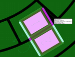
This picture shows what happens when the shapes are dynamic --> they are redrawn away from the pads of the component (if they are static, they aren't redrawn, but they register as DRC errors). The goal here is to have the shape that pin 2 of the capacitor is sitting on be Ground.
I have been able to import the drawing onto the etch layer and make the shapes dynamic, but I am having difficulties assigning them to nets. Originally, after importing the drawing, the shapes were static. I selected all the shapes, and used "Shape --> Change Shape Type" to convert them to dynamic. However, the "Assign net name" portion of the options tab in the editor is grayed out. The shapes are all assigned to "Dummy Net," and can't seem to be assigned to anything else.
I don't particularly care if the shapes are static or dynamic -- I just need to be able to assign them to nets. Does anyone have any advice/tips?

This picture shows what happens when the shapes are dynamic --> they are redrawn away from the pads of the component (if they are static, they aren't redrawn, but they register as DRC errors). The goal here is to have the shape that pin 2 of the capacitor is sitting on be Ground.
