deba_fire
Full Member level 3

Hi everyone,
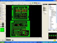
I recently did a PCB board and have few questions which are lingering in my mind.
Let me put down my routing strategy(placement done),
First fanout all the SMD components to make good pwr and gnd connection through vias.I think this was my first mistake ,as near the chip I had lot of power and gnd pins,which after fanout blocked the exit of other signals.I think auto fanout board creates lot of problems for SM chips(specially chips with very small pitch).How should we make sure that for the IC the tool uses only smaller vias?After fanning out board,I routed critical nets(differential signals,clock etc.) and locked them.Then I just used auto router hoping it will finish the routing of all other nets.But to my surprise it created lot more problems.Then I had to route other signals manually.I think auto router should never be used.
People who have experience in PCB layout please comment.Is there a good strategy which we should follow to route a PCB?specially packages where the pins are closely placed.What should be the first step in routing a board?what type of vias to be used for densely placed chips?What track lengths should be used near these chips?I am new comer to this field so if my questions are stupid please forgive me.
Regards
DB


