Continue to Site

Welcome to EDAboard.com

Welcome to our site! EDAboard.com is an international Electronics Discussion Forum focused on EDA software, circuits, schematics, books, theory, papers, asic, pld, 8051, DSP, Network, RF, Analog Design, PCB, Service Manuals... and a whole lot more! To participate you need to register. Registration is free. Click here to register now.

Bandgap deviation between simulation and tape-out

Status
Not open for further replies.

hktk

Junior Member level 3
Joined
Feb 2, 2005
Messages
27
Helped
2
Reputation
4
Reaction score
1
Trophy points
1,281
Activity points
263
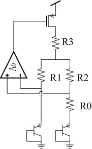
the simulation results of BG is around 1.22 but the tapeout results is 1.3~1.4. The structure is common, but L=2u for current mirror and W=2u L=30u for Res. Can any body give me some suggestion for the huge deviation between simulation and tapeout?
85_1287496886.jpg


---------- Post added at 14:07 ---------- Previous post was at 14:05 ----------

R3 will save area of chip, but at same time R3 will amplify Vos of Opamp to reference voltage.
 

Begin with the likely case that the substrate PNP is poorly
fitted and barely process controlled. Take some diode curve
data and see how well you match simulation I-V at the
operating point (and maybe 1 decade on either side, of
both current densities).

Then you can look for things like R0/R1 offset (op amp
gain / Vio - how many samples have you seen, to say
whether this is an anecdote or the norm?).

I don't know why R3 would save chip area, you can make
the FET throttle to the same net headroom and use a
smaller FET besides, if you left R3 out.

There could be litho effects if your big PNPs are not dummied
(presumably the single small one is in the center of the nest).

But my money's on the PNP modeling. If you trusted a digital
foundry analog model, without pulling your own curves, shame
on you.
 
  • Like
Reactions: hktk

    hktk

    Points: 2
    Helpful Answer Positive Rating
Hi hktk,

How many samples have you measured? An output voltage variation equal to 80 mV – 200 mV, (as you commented) can happen if the error-amplifier presents a significant offset voltage.
Have you simulated the expected offset voltage? Have you simulated it using monte-carlo and corner models?

Regarding the last BGR I simulated, I expected an output voltage variation equal to around +or- 30 mV (3-sigma), but I took into account a lot of precautions to reduce the offset voltage, to make a good layout, and ensure all transistors in saturation.
 
  • Like
Reactions: hktk

    hktk

    Points: 2
    Helpful Answer Positive Rating
1) Vref = Vbe+delta-Vbe*(R1+2R3)/R0, R3 can save chip area compare to the design that r3 is split into two individual Res;
2) BJT model is not the problem because another bandgap is good by using same bjt;
3) 10 samples was tested and the voltage variations are +80mV ~ +200mV, monte-carlo and corner analysis showed small variation.

Now I'm doublting the layout style, the current mirror is matched by finger, increasing the offset of the OP. Shame on me.
 

Hi hktk.

One could argue about the voltage shift caused by packaging, but the variation caused by this process is smalll (~ + or - 10 mV).
As you told about the layout style, I´m still think that this variation is caused by the op-amp offset.
But it is strange for me because Monte Carlo analysis does not take into account the layout style. Techniques like common centroid, interdigitated, dummies devices, and so on, tend to reduce the impact of variability.

Maybe this variation is something related to your measurement setup.
Are you using a printed circuit to bias your circuit? Probe station?
 
  • Like
Reactions: hktk

    hktk

    Points: 2
    Helpful Answer Positive Rating
I test my bandgap after package in pcb and osilloscope.

BTW, the reference voltage is connect to PAD by RC filter.

---------- Post added at 12:43 ---------- Previous post was at 12:04 ----------

The passive probe will introduce extra current for the test PAD, will it shift the bandgap output?
 

If there is significant ambient AC noise, you could see some
charge pumping. Ground loops between 'scope, meter,
supplies can induce large common-mode voltages that
are then "mostly" removed by instrument differential inputs.
If you probe (say) the ground plane with a 'scope probe
that has the ground clip detached, and see volts of 60Hz
(50Hz?) you do not have a quiet bench and are asking a lot of
your instruments.

The probe impedance could cause a resistive division against
the internal source resistance outward of the feedback loop.
But that ought to tend to lower, not raise the output voltage.

When you say the same transistors worked OK, is that same
wafer, different cell or a different wafer lot? Same transistor
core layout style or different? Breaking down the bandgap
into functional segments and looking at differences or lack,
might help you focus on the likely actors.
 
Hi hktk,

The “extra current” for the passive probe should be very low, and I think that is not the responsible. I thought that may have some problem with your PCB: noise, supply voltage, parasitic resistance and caps, etc.
It is needed to check all possibilities. It is difficult to say a straightforward explanation.

If you had one unpackaged sample, it would be possible to eliminate the hypothesis regarding the PCB.

please, If you have news during your investigation, post it and we can have discuss more about it. I´m also curious to know what it is happening.
 
  • Like
Reactions: hktk

    hktk

    Points: 2
    Helpful Answer Positive Rating
Leackage is found in this slot, and are there any methods to do failure analysis?
 

Hktk,

Where have you found leakage? Is your power consuption higher than you expected?
please, could you clarify your question about failure analysis?
 

If you knew the nature of your leakage, you might try to
add this feature to your models and see if the behavior
replicates. Of course everything leaks, the question is
how much, and what form (resistive, a current floor, or
simply subthreshold slope and VT not putting you on that
floor by VGS=0). None of this gets modeling departments
excited. You're probably on your own.

Similarly the PNPs' nonideal characteristics are not
to be trusted. Do you even have a WAT spec for any
attribute that speaks to how you use them? Such as,
multiple Vbe and hFE measurements that enclose the
range of current where you are working? If you did,
you could see whether they bear any relation to how
the bare devices simulate under the test conditions.

These are questions you could ask your foundry or,
if you have any, your device engineers (who may know
better where to look and who to ask).
 
Hi dck_freebird,

Please, if possible, could you clarify your point regarding:

1) “Similarly the PNPs' nonideal characteristics are not
to be trusted. Do you even have a WAT spec for any
attribute that speaks to how you use them? Such as,
multiple Vbe and hFE measurements that enclose the
range of current where you are working?”

In case the designer does not have access to silicon results (only access to the electric model): what would you suggest to overcome these not reliable models?

2) “But my money's on the PNP modeling. If you trusted a digital
foundry analog model, without pulling your own curves, shame
on you.”

What do you mean with “pulling your own curves”? Using the electric models? If the models are not reliable, how can this simulation help the designer?

Thank you very much,
 

If possible, you would like a few samples of a PCM test coupon,
a modeling test vehicle, something with the device you mean to
use. Then you take data (Gummel, and ideally some in the bias
condition you plan to use since Gummel is a not-useful circuit
configuration) that you can turn into things like a transdiode
log I-V (useful to assess the linearity of the real diode I-V
across decades of range, which is essential to the bandgap's
PTAT ideality) and beta-vs-IC with VCE=VBE (one way the
diode will slide off from expected - the beta is what idealizes
the transdiode and strongly influences the "Vf" (much lower
than the plain drain-well junction will read, because collector
current is most of the "diode" current).

You are interested in how real data (off a semiconductor
parameter analyzer like HP4145, 4156, ...) compares to
what the CAD system coughs up. And particularly at small
device sizes, periphery effects can make this vary a lot.
The base (well) surface in a CMOS process has only to "not
invert", as far as the process guys know or care. But if you
use it as a BJT, if it even moves a bit toward depletion then
the surface region takes more of Ib and then loses it to
surface recombination, killing low current beta and raising Vf
away from the ideal line. You might have need of field plating
to make it bend the right way, all that kind of thing. You might
want a "walled base" to force current flow vertical, despise
that this hurts Rc (by added distance) and device size. And so
on. On a "freebie" device like this, groundrules may be "what
will print" more than "what is best".

This is what you want to know. How much to believe the CAD
results. Because the final exam is a much more expensive
place to learn the lesson.

Even when you own the foundry, you may not "own" the agenda
of the modeling group. I know designers who have had to make
their own veriloga models for bandgap diodes, because they see
errors and can't get them fixed, even with data in hand. I have
borrowed their models because they work right and the "released"
models don't.

In any case you should begin with your foundry's application or
customer engineering folks. You may be the 37th guy to ask the
question and it merely never got pushed into the PDK docs /
models. Or maybe you are the first, and get to discover
something. Lucky you.

If you are a real customer with a real PO and a NDA in place,
there should be no problem getting you samples off some batch
of unshippable (hopefully for a reason unrelated to your interests)
wafers. Work the system.
 
Last edited:
Hi dck_freebird

Thanks for your reply.

What does mean "VF"?
are non-reliable BJT models only from digital process?
Or do you think that is common to find erros in BJT models in Analog/RF process?
 
  • Like
Reactions: hktk

    hktk

    Points: 2
    Helpful Answer Positive Rating
VF = "diode" forward voltage.

BJT models are something that a modeling engineer
assigned to a digital process, might not care about in
fine detail. Or be told not to. Fitting the low current
density and near-saturation regions is always tricky
and process-variable. If the thing is only tested at one
collector current then the fit of both Hfe-Ic and Vbe
could be crude. You just don't know, and that is the
problem here.

If you are using a designed device in a mixed signal
flow, you would expect more attention to detail. An
opportunistic device in a digital CMOS flow, all bets
are off.
 
Status
Not open for further replies.

Part and Inventory Search

Welcome to EDABoard.com

Sponsor

Back
Top