Julian18
Full Member level 3

Hi, everybody
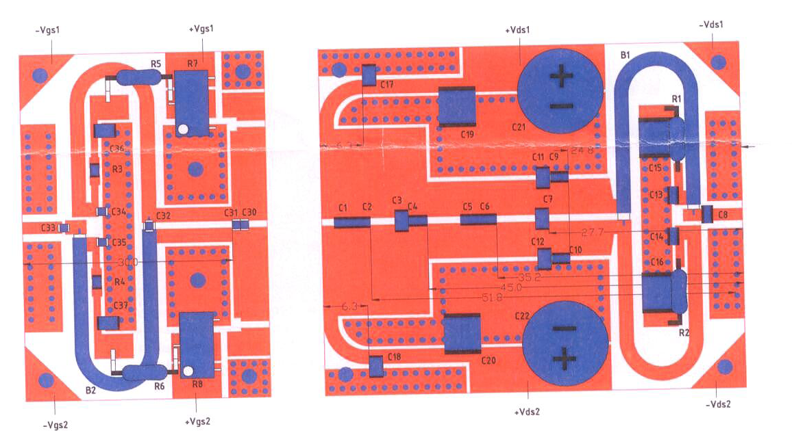
I am a newbie to the area of PA design or more general MW circuit design, although I have a bit of circuit knowledge. Now I am involved in a PA project which uses a NXP LDMOS as the transistor, but I think the circuit is too involved for me. the figure below is the demo circuit shown in the NXP application note.
Now here are my questions:
1. How to design the coaxial baluns at the input and the output.Why do we have to bend it? to save the area or to achieve some other goal?
2. since the balun is "unbalanced", can we erase the microstrip lines? (the micrstrip lines have the same shape as the co-axial balun, only are mirrored around the horizontal line)
3. how to specify the width and length of the matching transmission line? I see a lot of matching networks that are composed of transmission lines paralleled by some caps. but they all have the same width or characteristic impedance. so, why use three section of transmission lines with different width here in the input matching network? for the reason of saying area or some other more fundamental ones?
4. the forth one goes to the biasing network
why does the biasing at the output has round corners connecting to the drain of transistors? to implement inductors? if so , how to design them
Best Regards
Julian


