Continue to Site

Welcome to EDAboard.com

Welcome to our site! EDAboard.com is an international Electronics Discussion Forum focused on EDA software, circuits, schematics, books, theory, papers, asic, pld, 8051, DSP, Network, RF, Analog Design, PCB, Service Manuals... and a whole lot more! To participate you need to register. Registration is free. Click here to register now.

A little help breaking down circuit diagram

Status
Not open for further replies.

infinite_gbps

Member level 3
Member level 3
Joined
May 11, 2009
Messages
59
Helped
0
Reputation
0
Reaction score
0
Trophy points
1,286
Visit site
Activity points
1,804
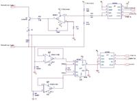
So I wanted to just get a better understand on what I am looking it with this application note.

My question is, where is this 4-20 mA current coming from in this circuit. I know the current (they tell me if you click that link) that flows through R3 causes a voltage drop across R3 and this drop also appears RS but what is actually supplying this output "loop" current? The OpAmp?

Picture of App Note from Analog Devices:
https://www.analog.com/en/verifiedcircuits/CN0009/vc.html
**broken link removed**

Just a side question, when I Pspice this I could never get the non-inverting input of the OpAmp to be close to zero. It's always has some higher voltage like 2.5V compared to the inverting input that has nV.
 

I was not very familiar with how current loop signaling works either but here is what I have figured out. Pretty interesting circuit and somewhat confusing at first. A little background is in order (I learned some from the app note)

Because the current level is what determines the logic level, the voltage level on the loop is unimportant. That is the 7 to 36V supply you see. The transmitter circuit, like in this schematic and typical of loop signalling, gets power from this variable supply. This schematic shows a voltage regulator which generates 5V from the variable 7 to 36V and uses the 5V to power the DAC and the opamp.

I attached a simplified schematic to better show what's happening. Firstly what is called PCB ground is not actually 0V relative to the loop supply ground. PCB ground will vary and be above loop supply ground (earth ground).

The opamp configuration is a classic voltage-to-current converter. The negative terminal will be driven to equal whatever voltage is on the positive terminal. You can see that the negative terminal=PCB ground. If the op amp is working correctly, the voltage across R3 will equal the voltage across RS.

If the DAC outputs 0V (relative to PCB ground) there will be 5V across R2, generating 5uA. That 5uA causes 394mV across R3 and because of regulation also causes 394mV across RS and 3.94mA to flow through RS. So when the DAC signal is 0V, the loop receives 3.945mA of current .

If the DAC outputs 5V, both R1 and R2 conduct current, which is 5uA + 25uA. Same principle applies and approximately 20.9mA curent flows to the loop.

Can you see how the PCB ground rises and falls to whatever voltage is needed to force the loop current?

The reason 4mA is chosen for zero logic instead of 0mA is because if you can still pass current around the loop even during a zero logic state, you can always power the transmitter from the loop supply voltage (so long as the transmitter, DAC and regulator does not require more than 4mA)

**broken link removed**
 
You were a huge help!

I read the application note but was not understanding how the regulation was happening and thought that PCB ground was zero.

So now PCB ground is just some reference for everything else, correct? I can actually try to Pspice the circuit you have in the attachment.

Will the choice of load resistance matter? From the way you explained it it shouldn't.

How would I change this circuit to do 0 mA to 20 mA? I'm pretty interested in that. Because I would be interested in using this as a 4-20 mA current receive as well. I already know how to do the receive circuitry and I have it across RS. If you take a look at the picture attached. I would want to be able to do 0-20 mA drive from the circuit and then be able to sum how turn it off. I know my receive section works because I tested it but all together it probably won't due to the drive circuitry always transmitting.

I really appreciate the help.


Added after 4 minutes:

I forgot to ask, where is the current coming from the OpAmp and through the BJT or is it coming from the loop supply voltage?

Some one on another board said it was loop supply voltage but though that was not the case and that this driver circuit was acting like the current source.

Sorry for all the questions.
 

The RL is not important, and it varies because you never know what the loop length is. Because of current signaling RL does not matter (but you need enough voltage available to get 20mA)

The PCB ground would be the ground reference for all the signaling circuitry, but I would not make it node 0. You should make node 0 the loop ground like shown in the app note. Take a guess at the RL and add some amount to see the real behavior.

the R2 sets the zero current so you could remove it to get 0mA. It seems that you are powering your transmitters from a local power supply rather than the loop voltage, so there is no problem.

One note is that 5V supply needs to have the negative terminal not tied to earth ground. It needs to float. Most power supplies are rated to float a certain voltage above ground.

Almost all the signal current flows from the loop voltage through the BJT. Microamps come from the rest of the circuits, but it all flows through the loop and comes from the loop voltage.
 
So if I remove R2 I will get zero milliamps, I see.

The million dollar question will be if I wanted to be a receive circuit like I have above, and I set my DAC to zero volts it does not seem like I would be able to see, for example, 4 mA coming from the loop supply across RS, i.e. being a receive circuit. Am I correct in this assumption?

The goal is to be able to configure for both Tx and Rx. I want to be able to have what ever current in coming in to flow across RS to read it back through a ADC like pictured.
 

Status
Not open for further replies.

Similar threads

Part and Inventory Search

Welcome to EDABoard.com

Sponsor

Back
Top