Warlike
Junior Member level 3

- Joined
- Dec 6, 2006
- Messages
- 31
- Helped
- 2
- Reputation
- 4
- Reaction score
- 0
- Trophy points
- 1,286
- Location
- Moscow, Russia
- Activity points
- 1,515
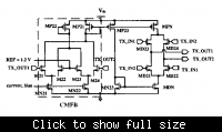
Hi! I design LVDS transmitter. Power supply is 2.5, transistors with thick oxide. Layout is standart: 2 nmos switch, 2 pmos switch, bandgap, bandgap based current reference and CMFB.
In DC this work good: Vos stable. Vol Voh also.
But when modeling transient process there are distortion at the moment of switching. Vos, Voh, Vol go up or down about 50-100 mV.
At the gates of the current source and sink there are also distortions about 20-30 mV.
Source and sink in the saturation region (Vds ~ 1 V). Swithes are in triode region (Vds ~ 70 mV for pmos and ~30 mV for nmos)
What can it be? Are it a bad CMFB, bad matching of transistors, parasitic capacitance or something else?
Tell please about base principle of LVDS driver design.
One more question. What is LVDS predriver? Now i use level shifter (from 1.8 to 2.5) and 2 chain of invertors to equalize V+ and V-. It is predriver? Or predriver is a something else?


