Continue to Site

Welcome to EDAboard.com

Welcome to our site! EDAboard.com is an international Electronics Discussion Forum focused on EDA software, circuits, schematics, books, theory, papers, asic, pld, 8051, DSP, Network, RF, Analog Design, PCB, Service Manuals... and a whole lot more! To participate you need to register. Registration is free. Click here to register now.

Understanding the circuit of flyback power convertor

Status
Not open for further replies.

bittware

Full Member level 4
Full Member level 4
Joined
Apr 3, 2004
Messages
208
Helped
1
Reputation
2
Reaction score
1
Trophy points
1,296
Activity points
1,986
Hello experts,
I am learning the flyback power convertor circuits. But I am quite puzzled by the attached circuit. There are seven red circles in question. Could anybody explain what these components are meant for? The nominal input voltage is 24VDC and output is 36VDC.
Thanks in advance.

Best regards,
bittware

Added after 1 minutes:

the circuit diagram download link
 

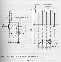
2,3,5 are the snubber network
**broken link removed**
http://www.fairchildsemi.com/an/AN/AN-4147.pdf

7 - the TL431 act as a error amplifier and reference voltage. So this circuit is a part of a feedback loop and determine the output voltage.
http://www.iele.polsl.pl/elenota/Hitachi/e204049_ha17431.pdf
**broken link removed**


6- C810 provides a short path to this current, thus preventing this HF common
current flowing other ways and creating EMI issues.
**broken link removed**

4-
**broken link removed**

1 - input filter
 

    bittware

    Points: 2
    Helpful Answer Positive Rating
Thanks, jony130.
But the first and 6th link are dead. Could you attach them on this website?
 

Well the first link work for my, 6th now is ok.


first jpg show how the snubber works.

When Tr is on Cr discharge through Tr.
When Tr is off Cr is charge trough Lp.
 

Status
Not open for further replies.

Similar threads

Part and Inventory Search

Welcome to EDABoard.com

Sponsor

Back
Top