Continue to Site

Welcome to EDAboard.com

Welcome to our site! EDAboard.com is an international Electronics Discussion Forum focused on EDA software, circuits, schematics, books, theory, papers, asic, pld, 8051, DSP, Network, RF, Analog Design, PCB, Service Manuals... and a whole lot more! To participate you need to register. Registration is free. Click here to register now.

Source Follower (OPAMP output stage)

Status
Not open for further replies.

sykab

Member level 2
Member level 2
Joined
Apr 26, 2008
Messages
44
Helped
0
Reputation
0
Reaction score
0
Trophy points
1,286
Activity points
1,579
Hi,

I'm using a souce follower, as you can see in the image, to do the output stage of an OPAMP.
I put a NMOS and a PMOS, that are, in the image, M2 and M1, respectively.
Am I right? I hope so, because it works and the opamp works well.
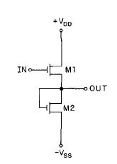
95_1210330781.jpg
 

the topology as such does not have any problem... if ur able to catch ur specs its fine.!!

sorry dear I missed ur point stating M1 is PMOS and M2 is Nmos...

dont you think ur making a common source stuff instead of common drain?

pmos :- what ever terminal is connected to vdd is source

nmos :- whatever terminal is connectdto vdd is drain...

See if ur trying to implement a source followr then ur driving Tx should have its source as output node... now decide accordingly which should be Nmos And which one shud be Pmos...


hope i made myself clear
 

    sykab

    Points: 2
    Helpful Answer Positive Rating
It can work. but I don't think it is good, because the liearity of it will be limited.

I think Source follower should be tow NMOS or Tow PMOS.
One is the current source and the other is the gm stage.
 

    sykab

    Points: 2
    Helpful Answer Positive Rating
sykab said:
Hi,

I'm using a souce follower, as you can see in the image, to do the output stage of an OPAMP.
I put a NMOS and a PMOS, that are, in the image, M2 and M1, respectively.
Am I right? I hope so, because it works and the opamp works well.

95_1210330781.jpg

it is ok, but the low voltage output cant reach the rail.
 

    sykab

    Points: 2
    Helpful Answer Positive Rating
For source follower, M2 is usually connected to a current mirror, right?
 

    sykab

    Points: 2
    Helpful Answer Positive Rating
Source follower should be two NMOS or two PMOS usually.
and one is for current source, and aother is for gm stage.
And this structure will limit the liearity.
 

    sykab

    Points: 2
    Helpful Answer Positive Rating
The topology is very good. I have also used it a while ago. But to realize the current source, other topologies can be used.
 

    sykab

    Points: 2
    Helpful Answer Positive Rating
For source follower better we have either 2 nmos or 2 pmos.
One of them can be used for fixing the current (and hence the current through input transistor) and nother can be used as input transistor. As the current is constant Vgs will be same and Vs (output node) will follow the Vg (input node). Thus we get an ideal gain of 1. We can avoid adding non linear effect with a current source or compromise that by using a resistance for load.
Depending on input range use nmos or pmos.
Hope this helps.
 

    sykab

    Points: 2
    Helpful Answer Positive Rating
Sadegh.j said:
The topology is very good. I have also used it a while ago. But to realize the current source, other topologies can be used.

Can you give me some examples of other topologies?

Thanks:D
 

well, basically, any current source topology will do it. You might want to use a normal current source composed of two transistors or you might even want to try something more complicated like Wilson or..... .

Please let me know if you want more help.

Cheers
 

    sykab

    Points: 2
    Helpful Answer Positive Rating
This is a tricky one, first I was confused becaus it looks like a Commo Source stage, and I would still say it is a CS stage. But if the nmos is sized rigth ( Output res should be 1/gm and gm_p=gm_n) than you got a gain of one (if the res_p is larg). The CM is set by the current and W/L ratio of the NMOS.And I think the NMOS has to be in diod conection becaus only here you have the r_out = 1/gm. I'm not sure but, if the transistors have the same gm/Id the gm will move equal and so the gain will keept constant. Actually it is a cool cercuit, make sure both transistors has the same Gm/Id.

Added after 6 minutes:

sorry did a mistake, the gm/Id of the diod can't be constant, so your gain will change.
 

    sykab

    Points: 2
    Helpful Answer Positive Rating
Status
Not open for further replies.

Similar threads

Part and Inventory Search

Welcome to EDABoard.com

Sponsor

Back
Top