Continue to Site

Welcome to EDAboard.com

Welcome to our site! EDAboard.com is an international Electronics Discussion Forum focused on EDA software, circuits, schematics, books, theory, papers, asic, pld, 8051, DSP, Network, RF, Analog Design, PCB, Service Manuals... and a whole lot more! To participate you need to register. Registration is free. Click here to register now.

How to draw the layout of Half adder

Status
Not open for further replies.

vlsitechnology

Full Member level 5
Full Member level 5
Joined
Nov 1, 2007
Messages
263
Helped
21
Reputation
42
Reaction score
14
Trophy points
1,298
Activity points
2,837
half adder schematic

Can anyone tell me the details of drawing the layout of half adder?

Added after 45 seconds:

I need to know the details without taking the spice levelnetlist
I mean with the help of boolean expression how can we draw the layout
 

half adder layout

Its quite simple. The equations for sum and carry are

sum = a xor b
carry = a and b

assuming a and b are inputs.

To implement xor:

sum = a xor b. CMOS logic is inverting logic. So you can do it this way.

sum = a xor b = (a xnor b)`

a xnor b = a`b` + ab

sum = (a`b` + ab)`

split a`b` as (a+b)'

sum = ((a+b)' + ab)'

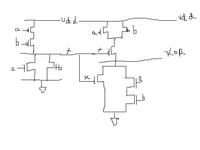
This can be implemented using an OR gate and AOI 12 gate.

The carry would be an and gate.

Let me know if you need any further information.

-Aravind

Added after 9 minutes:

This is the schematic


Added after 1 minutes:

You can probably work your way through the layout with the schematic. Let me know if you have any doubts with the layout.
 
cmos half adder

Dear VLSI technology,

U r asking how to draw a layout of half adder.

Fine u need a layout tool.

u need a transistor level(CMOS level) design of the half adder.

That cmos should be of certain technology.

Then it cmos level transistor should be designed properly like consedering its

parameters such that we should get any violations.

if we get we need to adjust.

If we get certain width, in layout we need to keep the polysilicon area of that width.

then start layout by placing active n- well p diffusion, bulk connection, keep the lenght according to technology and width u designed then connect drain source gate as per requrinment then connect VDD, VSS , then connet onter connection then tap out i/o ports , finally create a abutment box ant if u want place in library place.

hope u understand
santu
 
half adder circuit using cmos

use orcad, make schematic of whatever you want (gates only), create the verilog file .

using mirowind you can convert the verilog file into the layout !

enjoy !
 

Status
Not open for further replies.

Part and Inventory Search

Welcome to EDABoard.com

Sponsor

Back
Top