Continue to Site

Welcome to EDAboard.com

Welcome to our site! EDAboard.com is an international Electronics Discussion Forum focused on EDA software, circuits, schematics, books, theory, papers, asic, pld, 8051, DSP, Network, RF, Analog Design, PCB, Service Manuals... and a whole lot more! To participate you need to register. Registration is free. Click here to register now.

subthershold conduction,weak and strong inversion

Status
Not open for further replies.

maalma

Member level 1
Member level 1
Joined
Mar 1, 2007
Messages
36
Helped
0
Reputation
0
Reaction score
0
Trophy points
1,286
Location
Morroco
Activity points
1,495
hello all,
i have some trouble in understanding the subthershold conduction, we are bellow Vt but we have a conduction?? can you please give me more details?
what is the difference between weak inversion and strong inversion?? how can we explain it??
 

weak inversion is when surface potential (phi s) <2(phi f)
strong inversion when phi s > 2(phi f) + thermal voltage
 

    maalma

    Points: 2
    Helpful Answer Positive Rating
Hi,
Conduction current changes 10 times by change in the Vgs by one subthreshold slope.The subthreshold slope of a typical device is 60-70mV.
Regards,
Jitendra Dhasmana.
 

    maalma

    Points: 2
    Helpful Answer Positive Rating
Subthreshold conduction occurs (the name says it) when Vgs < Vt. Then the MOSFET
behaves like a bipolar transistor. This effect occurs only when Vds is a few hundred mV.

So:

Id,subtr = I0*exp(Vgs/k*Vt), whereas k is a nonideality constant - depending on the process I guess.
 

    maalma

    Points: 2
    Helpful Answer Positive Rating
Hi,
Let's consider the MOS operation.
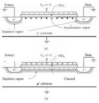
By applying a negative voltage to the gate and increasing its absolute value (part a in the figure) the positive charge is attracted to the channel region and the Accumulation region is formed right under the gate oxide.
By applying a positive voltage to the gate and increasing its value slowly, negative charge is attracted to the channel region and a channel is gradually formed under the gate oxide. When Vg >> 0 we call it the strong inversion (part b in the figure). This negative channel can conduct between Drain and Source.


The gate-source voltage, for which the concentration of electrons under the gate is equal to the concentration of holes in the p- substrate far from the gate, is commonly referred to as the transistor threshold voltage [Johns, Wiley, 1997].
Under the threshold voltage a few electrons exist in the region and so the conduction occurs. But it is not strong. We call it Weak inversion.
For more information you can refer to books like Johns or Gray.
 
Status
Not open for further replies.

Similar threads

Part and Inventory Search

Welcome to EDABoard.com

Sponsor

Back
Top