Continue to Site

Welcome to EDAboard.com

Welcome to our site! EDAboard.com is an international Electronics Discussion Forum focused on EDA software, circuits, schematics, books, theory, papers, asic, pld, 8051, DSP, Network, RF, Analog Design, PCB, Service Manuals... and a whole lot more! To participate you need to register. Registration is free. Click here to register now.

Die size and Core size

Status
Not open for further replies.

designer_ec

Member level 4
Member level 4
Joined
Mar 31, 2007
Messages
68
Helped
1
Reputation
2
Reaction score
0
Trophy points
1,286
Activity points
1,752
die area, core area

Please anybody tell me that in P&R when we are doing floor plan how to decide Die size for chip level and how to decide core size.Please inform me if there is any formlas to calculate those sizes or if any thumb rule for that calculation.
 

die size core size

you can search this website for this topic!
in principle, it may be determined by the core area and the pad area!


br,

Thomson
 

calculate core size

quite simple.

1. core size = netlist area/estimated cell density
2. die size = core size + pad height + power ring width.
 

two more factors to determine the die size and core size.
-- core-limited design
-- pad-limited design
 

Hi Ray123,
Please describe the core limit and die limit.

Added after 3 minutes:

Hi ray123

Sorry,befor this I ask wrongly.
Please describe the core limit design and pad limit design.
 

if the number of input/output pads are more and to accommodate that, the chip size is determined, then, its pad limited.

if core area is high, and accommodating pads is not a problem, then, its core limited.

Added after 42 minutes:

you can get more information about core limited design and pad limited design in ASICs by sebastian smith
 

Check Out,

to eval the core area for a core limited design

a) check out the total # of signal pads required. Either it is obtained from front end or is determined from the knowledge of interfaces to the chip.
b) Total area occupied by the modules in the design is calculated. This area is often with respect to NAND equivalents. This is done as apart of calculation of minimum area of chip required.
c) Next step is to find increase in area due to
1) Scan replacement
2) Clock tree insertion
3) HFN on scan enable
4) HFN on async reset
5) Hold fixes on scan chain
6) Hold fixes in functional paths
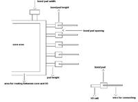
and calculate Pad overheads with the diagram shown here

or lese, to calculate pad area for a pad limited design check out the aspect ratio and by simple means, get the # of pads along length and breadth of the chip
Height or Width = ( Pad Width * No of pads + Pad Spacing + 2 * Corner Pad width)

Note: The corner pad width is to be taken only if its value > = to Pad Height + Bond Pad Height

Cheers

Added after 1 minutes:

Forgot the image

 
Thanks for all.
Hi Svr,can you tell me the what isHFN in below statements,which were given by you.
HFN on scan enable, HFN on async reset .
 

Status
Not open for further replies.

Part and Inventory Search

Welcome to EDABoard.com

Sponsor

Back
Top