Continue to Site

Welcome to EDAboard.com

Welcome to our site! EDAboard.com is an international Electronics Discussion Forum focused on EDA software, circuits, schematics, books, theory, papers, asic, pld, 8051, DSP, Network, RF, Analog Design, PCB, Service Manuals... and a whole lot more! To participate you need to register. Registration is free. Click here to register now.

How to calculate this voltage gain?

Status
Not open for further replies.

walker5678

Full Member level 3
Full Member level 3
Joined
May 17, 2006
Messages
179
Helped
7
Reputation
14
Reaction score
3
Trophy points
1,298
Activity points
2,493
calculation of voltage gain of transistor

HI

Attached picture is the circuit of a rail to rail differential input stage followed by a Class AB floating bias circuit. Anyone has the concept how to analyze and design the voltage gain of the point A and B, could you give some advice? Appreciate you help, thanks!
best regards.
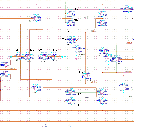
64_1168502694.gif
 

how to calculate voltage gain

the NMOS PMOS combination between A and B seems to like a Class AB control circuit. Also, there is an AC short between point A and B. You can convince yourself by doing proper analysis. Therefore, you can calculate the voltage gain of the amp as you would do regularly (i.e. calculate the gm of the input stage and the output impedance of the first stage and gm of the second stage together with the output impedance of the second stage and so on).

However, what you should keep in mind is that the gm of the input stage changes depending on the common mode input voltage. Gm of the input stage when your common mode is such that both the NMOS and PMOS pair are on is higher than when just the NMOS (or just the PMOS) pair are on.

HOpefully this helps.
 

    walker5678

    Points: 2
    Helpful Answer Positive Rating
calculating voltage gain

Thanks for the explanation.

Yes, the currents in the M7 and M8 do change in the complementary mode when there is AC signal added to the input stage. This is interesting, and i am just curious to know how this circuit structure make this. How to design the W/L size of M7 and M8?

Another interesting thing is that when VA decrease (output PMOS pull current from Vdd), the VB is kept to a minimum voltage (about 700mV), and when VB increase ( output NMOS drive current to GND), the VA is kept to a maximum voltage (about 4.1V, vdd=5V). What 's the purpose?


best regards/
 

how to calculate the maximum voltage gain

1. To your first question about sizing M7 and M8:
It is not difficult at all. M7 and the way you are biasing the gate of M7 (popularly done with just two PMOS diodes to Vdd) together with the PMOS output transistor forms a translinear loop. Therefore, once you decide on the drain current for M5 and M6 (and half of this current flows into M7 if biased properly), then with the translinear loop and M5 drain current you can set the Q current for the output PMOS. You have a similar loop on the N side. Therefore you can size the W/Ls for all these transistors. There is literature available. this type of class AB biasing is called a "feedforward" Class AB biasing.

2. The phoenomenon you are talking is one of the features of this class AB circuit. By keeping VB to a voltage when VA decreases you are thereby no longer providing an AC short between nodes VA and VB as they are decoupled. Instead, what you are doing is when the PMOS output transistor is driven hard, you are keeping a small amount of current flowing in the NMOS output transistor so that it is "ON". Therefore when a signal transition occurs from +ve to -ve (or vice versa), there is no cross over distortion. This min. current can also be derived by means of translinear loop analysis.

Hope it is clear. And, you make a good observation on the circuit!!!
 

    walker5678

    Points: 2
    Helpful Answer Positive Rating
calculate voltage gain

Thanks a lot , cellphone, your instruction make me more clear about this circuit structure.
 

Status
Not open for further replies.

Part and Inventory Search

Welcome to EDABoard.com

Sponsor

Back
Top