Continue to Site

Welcome to EDAboard.com

Welcome to our site! EDAboard.com is an international Electronics Discussion Forum focused on EDA software, circuits, schematics, books, theory, papers, asic, pld, 8051, DSP, Network, RF, Analog Design, PCB, Service Manuals... and a whole lot more! To participate you need to register. Registration is free. Click here to register now.

Help on understanding Power MOSFET DataSheet, IRF530

Status
Not open for further replies.

mengghee

Full Member level 3
Full Member level 3
Joined
Nov 29, 2005
Messages
163
Helped
8
Reputation
16
Reaction score
5
Trophy points
1,298
Location
United Kingdom
Activity points
3,105
power mosfet datasheet

Hiye everybody,

I have attached a datahsheet here and i am just wondering if anybody can help me understanding the IRF530 Datasheet. basicly my question is, in order to turn on the mosfet, what voltage should i apply to the gate ? and what sort of current ? and where can i find it in the datasheet ? thank you very much.

regards,
mengghee
 

mosfet datasheet

I did not see the attached datasheet -- but I am assuming that you mean
this one from International Rectifier
http://www.irf.com/product-info/datasheets/data/irf530.pdf

The important parameter is Vgs(th) -- the threshold voltage from gate-source.
Once you apply a voltage above this level, the FET should conduct. The parameter is on page 2, fourth item from the top. There is also Figure 3 on page 3 that plots this. You should also put some gate resistance RG as shown in the datasheet. The value of this depends on how fast you want to turn the device on. The gate charge characteristics are given in the datasheet as well.

I hope this helps you out.

Best regards,
v_c
 

    mengghee

    Points: 2
    Helpful Answer Positive Rating
mosfet rg

Hi,

Thanks V_C, sorry about the datasheet, i was about to link the datasheet but there was a problem with my pc. how can i choose the resistor value ? can you be more specific ? i don't understand the datasheet very well. I am working on a PWM signal that is working around 50Khz. thank you very much

regards,
mengghee
 

irf530

Usually the gate resistance is in the 100 ohm range, sometimes you have to experiment to see what you really need. It all depends on what your driving circuit is and what your MOSFET looks like.

Take a look at this document to get a better picture of what I mean http://www.analogzone.com/pwrt1208.pdf

Basically, if you make RG too small then your FET might turn on very quickly which might cause noise in your circuit. If you make RG too large, then the MOSFET takes a long time to turn on -- this will increase the conduction losses in the MOSFET. This is because we really want to use the MOSFET as a switch -- ON (saturation) and OFF (cutoff). If we turn it on slowly, then the MOSFET spends much more time in the LINEAR (ohmic) region and it acts like a resistor and burns up power at each cycle.

Also do a google search on "MOSFET gate drive circuits" -- you will find lots of information.

v_c
 

    mengghee

    Points: 2
    Helpful Answer Positive Rating
mosfet gfs

mengghee,

The place to start is the Gate-Source threshold voltage Vgs(th). Notice, however, that this parameter is the voltage at which the FET just starts to turn on. For the IRD530, this is specified at Id = 250 uA. Let's say you need an Id of 5A. From the definition of Forward transconductance, and using deltas instead of differentials, DeltaVgs = DeltaId/Gfs. For an Id change of 5A, and the specified minimum Gfs = 5.1, you need an additional Vgs of approximately 5/5.1 = 0.98V. In addition, to compensate for the fact that Gfs tends to decrease as temperature increases, I would add another 20%. So the additional Vgs would be 0.98 X 1.2 = 1.18V. Adding this delta to the worst case (high) Vgs of 4.0V, you will need a Vgs of 4 + 1.18 = 5.18 to guarantee full turn-on @ 5 Amperes (without smoke). You also need to ensure that you supply enough gate current to supply the gate charge, in the presence of Gate-Source capacitance and miller capacitance. As V_C mentioned, if the gate current is inadequate, then the FET will spend excessive time turning on and off, an dissipation will increase.
Regards,
Kral
 
  • Like
Reactions: jay1691

    mengghee

    Points: 2
    Helpful Answer Positive Rating

    jay1691

    Points: 2
    Helpful Answer Positive Rating
understanding mosfet datasheet

Hi guys,
If I want to use a fet as a switch with control voltages 0 and 5V do I have to care about the VGS-IDS relation? What if IDS of the load changes from time to time?
 

forward transconductance definition

thuvu,
As long as you supply a high enough Vgs to ensure that you can support the maximum expected current using worst-case (High) Vgs(th), Gfs(Low), and junction temperature (High) then you don't have to worry about the Vgs-Ids relation.
Regards,
Kral
 

    mengghee

    Points: 2
    Helpful Answer Positive Rating
mosfet,+rg

kral,

can you actually explain to me what Gfs means ? I have read it somewhere that it is the forward transconductance. but what does it actually do ? and thank you for the reply before. you have actually helped me a lot in understanding MOSFET. though my understanding towards it is yet to be perfect.

regards,
mengghee
 
irf530 circuits

gfs is the "gain" of the FET and has the units of Amp/Volt. Changes in gate-source voltage vgs times gfs gives rise to changes in the drain current.

You can think of the FET as a voltage-controlled current source. The controlling voltage is vgs and the multiplication factor is gfs.
 

    mengghee

    Points: 2
    Helpful Answer Positive Rating
how to read mosfet datasheet

mengghee,
I can't improve on v_c's explanation. It fits nicely with my previous reply on how to calculate the "Delta" Vgs.
Regards,
Kral
 

    mengghee

    Points: 2
    Helpful Answer Positive Rating
how to read a mosfet datasheet

thanks guys,

is there some sort of a calculation of formula where i can calculate the resistance at the vgs ? thanks

regards,
mengghee
 

calculate mosfet rg

Rgs can be calculated by looking at Cgs (gate source capacitance). The RC time constant determines how fast the gate charge (Qgs=Vgs Cgs) reaches the level it needs to turn on the FET. Cgs is not a constant but curves are given for different operating conditions on data sheets or gate charge characteristics might be specified.
 

    mengghee

    Points: 2
    Helpful Answer Positive Rating
ids mosfet datasheet

hiye everybody,

i have changed my mosfet as irf530 is not in stock. currently i am using stp50ne10.
i am building a 500mA boost converter so the current across it is 500mA. let me make Id = 1A in case anything happen.

Vgs=Id/Fgs where the minimum forward gfs stated is 20
= 1/20
= 0.05v
adding 20% towards it
Vgs= 0.05×1.2
= 0.06
so Vgs should be the worst vgs stated in datasheet + vgs calculated above

Vgs = 4+0.06
= 4.06

does that sound about right guys ? I have yet to calculate Rg. really appreciate u guys help. thank you

datasheet of the mosfet is in the link below

**broken link removed**

regards,
Jeffrey

Added after 28 minutes:

my understanding towards mosfet is getting better and better but still need some guidance.

assuming that my Vgs = 5V, through the datasheet 'Gate Charge vs Gate-source Voltage' curve, the gate charge is approximately 30nC.
so,

Cgs = Qgs/Vgs
=30n/5
=6nF

is the above correct ? but i am wondering, in order to get the Rg value, we need to specify the time constant isn't it ? what should i choose the time constant to be ? thank you again.
 
fet vgs=5v

First of all, let me say that the MOSFET you selected is way to powerful for your application. But that is beside the point. Let me answer your question.

I am going to assume your boost will be operating in continuous current mode (CCM).
That means that the output current is a trapezoid whose average over one switching period is the output current. What that means is that the peak MOSFET current is higher than the load current. How much higher?
Look at the picture. The MOSFET current is the blue waveform. The black horizontal line is the inductor average current (Iind), while the yellow one is the output current (Iout)
As you can see, the MOSFET actually carries the inductor current while on.

Now the output current is

Iout=Iind*(1-DC),

where DC is the duty-cycle and to a first approximation we eill consider it to be

DC=1-Vin/Vout,

where Vin is the input voltage and Vout the output voltage.

If your boost doubles the input voltage, then the DC≈0.5, which means (1-DC)≈0.5 so the MOSFET current you should use to calculate the on voltage drop is twice the output current, that is 1A.

Now to calculate the on voltage drop, you should use the Rdson given for the gate drive voltage you are going to use, typically 5V or 10V, depending on MOSFET rating. In your case you should use 10V. The Rdson max for 10V drive is 0.027ohm. But this value should be corrected assuming the junction temperature is 100C. As you can see from the normalized on resistance graph, at 100C it is about 60% higher than at 25C, that is 0.027*1.6=0.043 ohm.
So the MOSFET on voltage drop is:

Vdson=0.043*1A=0.043V

As for the gate resistor, it is chosen such that the switching time represents only a small fraction of the switching period. Let's say we set it to tsw=100ns.
This is the time it takes the MOSFET to transition through the plateau region of the gate charge characteristic (the flat portion in the middle).

You have calculated the actual Vgs voltage for your current as being 4.6V, instead of the 5V seen in the graph. With that, the gate-drain charge drops a little. Look at how much charge there is within the plateau region. From the graph, corrected to 4.6V by shifting down the plateau an stretching the left slanted portion, I would say it is about 40nC.

Assuming you drive with 10V, then the gate resistor will have 10V-4.6V=5.4V across it during the time the voltage is at the plateau. Then the current through the gate resistor is 5.4V/ Rgate
This current actually supplies charge to the gate and the MOSFET exists the plateau region once the 40nC have been supplied.
That means that Q=Igate*tsw
Igate=Q/tsw=40nC/100ns=0.4A

That is the gate curent, 0.4A. Thus, the gate resistor is Rgate=5.4V/0.4A=13.5 ohm. This is pretty much a typical value for such a large MOSFET.
 
  • Like
Reactions: jay1691

    mengghee

    Points: 2
    Helpful Answer Positive Rating

    jay1691

    Points: 2
    Helpful Answer Positive Rating
calculating rg for mosfet

can anyone tell me please, what is the disadvantages of using too powerful mosfet ? my university currently has stock on irf511. do you guys think that it is going to be more suitable ?? thank you.

regards,
mengghee

Added after 56 minutes:

can u guys also suggest a mosfet for me ? thank you
 

fet cgs

The only disadvantage is its high input capacitance, which leads to slow switching times, if you don't have a good driver, or it leads to higher power consumption for the gate driver, if you have a good one.
 

    mengghee

    Points: 2
    Helpful Answer Positive Rating
how to read mosfet datasheet mosfet

Hi, can I ask some basic questions?
if I am required to use mosfet as a switch, What are the data that i have to see on data sheet?
I want to design a switch that control the power supply to some device. This device requires 20V to turn on.

http://singapore.rs-online.com/web/search/searchBrowseAction.html?method=retrieveTfg&Nr=AND(avl%3asg%2csearchDiscon_sg%3aN)&N=4294862100+4294958788+4294832607&binCount=125&Ns=Vds%20max%20V&Nso=0#resultArrow

So If I am to choose which MOSFET to use, do I have to look at Vds max? am I looking at the right thing? Or I should more concern about the ID max?
 

what is the value of gfs for a mosfet

All maximum ratings have to be kept. Vds, Id, also possibly Pmax (steady state and transient)
For the switch application, rds,on is typically an important property, also the required Vgs.
 

Hi if i wa to use IRFz44n*2 Mosfet, in an inverter how would iwork work the power dissipation

thanks
 

Hi everybody

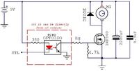
This is a very great thread! I also have similar questions with mengghee, and I find lots of answers in here. I want to make sure, if I am to drive unipolar 5Vdc(rating) / 0.4A(max) DC motor with IRF540 (the one available in campus), is the attached circuit and the Rg calculation below can be done?. The input signal is from either directly from microcontroller ATmega (max 40mA) or even Optocoupler (Imax=100mA).

Based from VVV and Kral's asnwers, determining Rg is;
1. deltaVgs = deltaId/Gfs(datasheet) = 0.4A/20 = 0.02V.
So Vgs = Vgs(max,datasheet)+deltaVgs*temp_compensation = 4V+0.02V*1.2 = 4.024V
2. Rds_on = 0.077Ohm for 10V.
At T=100degC, Rds_on = 0.077Ohm*1.6 (datasheet, curve) = 0.1232 Ohm
3. Switching time = tsw = 45ns (datasheet).
Because Vgs = 4.024V, Q = around 5nC (datasheet, curve)
Because the signal voltage = 5V, then voltage accross Rg = VRg = 5-4.024V = 0.976V
Ig = Q/tsw = 5nc/45ns = 1/9A.
So Rg = 0.976V/(1/9A) = 9.784Ohm

My questions:
1. Is this circuit and Rg applicable? Is there any other theoretical/practical consideration that I need to put into account?
2. I think the signal current (Ig=1/9A) will be too big to be handled by microcontroller (max 40mA) or even Optocoupler (AQW211, Imax=100mA), or is it?. Is there any way to reduce the Ig without reducing the performance?

Thank you for any help you can provide.

- MOSFET IRF540 datasheet: https://www.google.com/url?sa=t&sou...4JmPBA&usg=AFQjCNHWB1nHU__wqYgcz3-XNUeV4yQ-ZQ
- Motor datasheet (see T2-03 e-Compact): https://www.parker.com/portal/site/... - ULTRA-COMPACT DIAPHRAGM PUMP&vgnextfmt=EN#


Status
Not open for further replies.

Similar threads

Part and Inventory Search

Welcome to EDABoard.com

Sponsor

Back
Top