Continue to Site

Can I Run the JFET at 4.5 Volts in this 103 MHz Colpitts Oscillator Circuit?

Scarlett133

Newbie level 6
Newbie level 6
Joined
Jan 15, 2025
Messages
13
Helped
0
Reputation
0
Reaction score
0
Trophy points
1
Activity points
96
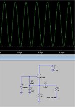
I was wondering if I could power my JFET Colpitts oscillator circuit with 4.5 volts with no issue, its an BF256B by Onsemi DATASHEET
If it doesnt work i could try an J310 or other JFETs

1741248860613.png
 
Last edited:
According to the LTspice simulation the oscillator works down to 2.2V.
 

Attachments

  • colpitts.jpg
    colpitts.jpg
    51.2 KB · Views: 48
Define works?

The current limit implies very low power.
--- Updated ---

Historically 100 MHz type Colpitts work down to Vcc=0.6V with a RF NPN BJT. The Clapp Osc can tolerate higher loaded Q values.
1741464543797.png
 
Last edited:
well i wanted to use an BJT At first but the Inductor would short the base to ground, i dont think that would work
 
It would work if you applied some bias to a BJT. The present design uses a JFET because it is a depletion mode device, it conducts without bias and applying gate voltage reduces Id. At the moment the gate is held slightly negative of the source because the voltage dropped across R1 makes the source more positive than ground. If you add a large(ish) DC blocking capacitor in series with the coil with value high enough that is doesn't adversely affect the tuning (say 1nF) and add bias resistors it should work fine, even at very low supply voltage.

Brian.
 
well i wanted to use an BJT At first but the Inductor would short the base to ground, i dont think that would work
The emitter is 0V but not the inductor. It is actually pulled up by the collector R. Do you need a simulation?

Can you please define "works" in Engineering specs? like impedance , current , amplitude, supply voltage. The better you define it, the better it gets.
--- Updated ---

This oscillator can be really difficult to get going without all the details of your layout. It can't be put on a breadboard for example unless you know what you are doing and the frequency will shift from stray inductance or ESL of 5 to 8 nH/mm and stray or even probe capacitance can ruin it since it is unbuffered.

So be patient and let us know what you need and what you have. (photos help on layout.)
 
Last edited:
It turned out like this for me
--- Updated ---

Ansoft Designer/ADS
 

Attachments

  • 1.jpg
    1.jpg
    98 KB · Views: 33
  • 2.jpg
    2.jpg
    73.3 KB · Views: 32
  • 3.jpg
    3.jpg
    105.1 KB · Views: 34
  • 1.jpg
    1.jpg
    140.5 KB · Views: 35
  • 2.jpg
    2.jpg
    61.7 KB · Views: 33
Last edited:
Looks good.

If you shift the impedances to lower C on gate and higher C on output, you may see a gain of 10 using 12 pF coupling. Reduce C1 by Cgs of JFET. Or it may not have enough loop gain with gm to oscillate and sensitivity to frequency increases.
If you have a PCB with this FET and components and no oscillation, then the FET may be low in gm or the actual values and stray ESL and C may be excessive or actual values not as shown.
1741926502310.png
 
Last edited:


Write your reply...

LaTeX Commands Quick-Menu:

Part and Inventory Search

Welcome to EDABoard.com

Sponsor

Back
Top