Continue to Site

Welcome to EDAboard.com

Welcome to our site! EDAboard.com is an international Electronics Discussion Forum focused on EDA software, circuits, schematics, books, theory, papers, asic, pld, 8051, DSP, Network, RF, Analog Design, PCB, Service Manuals... and a whole lot more! To participate you need to register. Registration is free. Click here to register now.

Identify DC gain and DC operations point of Floating inverter amplifier

Henry98

Newbie level 6
Newbie level 6
Joined
Jun 29, 2024
Messages
12
Helped
0
Reputation
0
Reaction score
0
Trophy points
1
Visit site
Activity points
191
Hello, everyone,
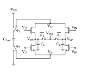
I want to identify DC gain and operations point a floating inverter amplifier as picture below, but I try run dc, ac, in ADE but I confuse about the result.
Anyone Could you help me the guideline to identify DC gain and operations point.
Thank, everyone
1727223376406.png
1727223516298.png
 
Hi @Henry98
Your dc/ac simulation wouldn't give you a valid result since your circuit is a switching circuit, hence identifying the dc/ac currents is impossible for a simulator.
I can recommend using PAC/PSS analysis (that we use for SC-circuits analysis for example) to get the desired result.
You may find the following tutorials useful (attached).
Hopefully, it helps.
 

Attachments

  • ATutorialOnAdvancedAnalysisForCadenceSpectre.pdf
    710.7 KB · Views: 97
  • PAC_analysis.pdf
    357.6 KB · Views: 73
Thank you, @sidun.av
Your answer is really helpful to me

I tried to simulate my circuit with PSS, PAC and then I have a result as below, Could you help me explain for me the meaning of that result?

This is my result at input harmonic -2:
1727311162200.png
1727311018643.png


with the input signal is 1.7k and switching frequency is 2MHz
and with setup of PSS , PAC as picture below:
1727311267921.png
1727311299593.png


Thank you
 
@Henry98 , you are getting a quite weird result...
1. Did you make sure that you have only 1 clock source in the circuit (and it has the highest frequency) and the rest are just derivatives of it?
2. Did you try to run transient analysis to make sure that you are getting an output signal which is close to what you are expecting? Apart from simulation settings, I am suspecting some errors in your schematic, so maybe that's why you are getting -6kdB (!) as a result.
3. It would be useful to see your schematic by the way...
 
Hi @sidun.av ,
1. My schematic is using a input voltage source is 2kHz, and two inverted source of clock 2MHz to control the switching of circuit.
2. when I run transient simulation, output is kind of like á my expected.
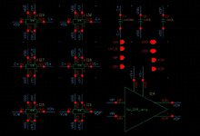
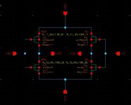
3. My schematic using in this simulation as picture below:
1727354055768.png


transient output of this circuit is:
1727354118799.png


And the voltage gain of this structure:
1727354182783.png
1727354206850.png


below í my setup for PSS and PAC:
1727354268800.png
1727354295023.png


Could you help me check it whether my schematic or setup of PSS , PAC is wrong?

Thank you.
 
The one thing I've noticed about your schematic is that you have more than one fundamental frequencies: CLK and CLK_B. I understand that this is just inverted clocks but I am not sure that the simulator can recognize that. Try implementing CLK_B by inverting a CLK through inverter and see if it gives you any meaningful result.
In a meanwhile, I will have look on your analysis setup and tell you if there is something wrong with it.
 
Hi @sidun.av,

I'm checking my circuit then I realized that Pmos, Nmos of my circuit went to region 0.
Therefore, I suspected that DC analysis can not identify the region of Tr of switching circuit because that circuit working in difference state for each of level (High/low) of clock.
Could you share me how to check operation point of TR in switching circuit?

Thank you.
 
I'm checking my circuit then I realized that Pmos, Nmos of my circuit went to region 0.
That makes complete sense, because in DC analysis (depending on the initial conditions of your circuit) some switches will be open leading to open circuit and no current flow.
My suggestion will be the following:
1. Perform a transient analysis;
2. Go to View->Annotations and select Transient Operating Points;
3. Specify the time when your circuit is at the phase 1 and inspect the operating points. Repeat the same for the time when your circuit is in phase 2.
 
Hi @sidun.av,

Thank you for your suggestion
In the meantime I set up cadence to do simulation again, I have some questions:

1: I read your guideline document, I wonder that why input voltage for circuit need to be DC voltage not AC voltage to run PSS.
1727425978530.png


I also reference to this video and realized that they also change from input AC to input DC to run PSS and PAC
1727426156432.png


my circuit is using AC input to run PSS, I think maybe it also is one of problems that I need to fix.
Thank you.
 
This is not how a forum is meant to work.

Please do communication in public.

Klaus
Hi @KlausST ,
I understand that. I will post the document, but I wanted to get some feedback first on its correctness and accuracy. Moreover, I didn't expect it to be in such demand to be honest.
 

Attachments

  • PAC-analysis.pdf
    230.3 KB · Views: 7
Well, I want to design a floating inverter amp for delta sigma adc. I don't know how to simulate accurately and whether my simulation method is correct. Another point is that I can only think of testing its gain, but I don't know what other important features of FIA need to be considered.
 

Attachments

  • FIA.png
    FIA.png
    16.1 KB · Views: 11
  • fiasch.jpg
    fiasch.jpg
    246 KB · Views: 11
  • cmosinv.jpg
    cmosinv.jpg
    141 KB · Views: 10

LaTeX Commands Quick-Menu:

Similar threads

Part and Inventory Search

Welcome to EDABoard.com

Sponsor

Back
Top