Continue to Site

Welcome to EDAboard.com

Welcome to our site! EDAboard.com is an international Electronics Discussion Forum focused on EDA software, circuits, schematics, books, theory, papers, asic, pld, 8051, DSP, Network, RF, Analog Design, PCB, Service Manuals... and a whole lot more! To participate you need to register. Registration is free. Click here to register now.

My t flip flop is not working

mssong

Junior Member level 2
Joined
Jul 25, 2023
Messages
22
Helped
0
Reputation
0
Reaction score
0
Trophy points
1
Visit site
Activity points
190
My t flip flop is not working.

It could be a very simple problem.

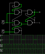
Below is the schematic of the t flip flop and on the right is the simulation result.

I have an input of 1, and I need to create a logic circuit that changes the signal level of the previous stage from 1 to 0 or 0 to 1 whenever CLK comes in, so I decided that a T FLIP FLOP would be a good choice, but it doesn't work.

What is the problem?
1725271953731.png
1725272039457.png
1725272115260.png

--- Updated ---

My t flip flop is not working.

It could be a very simple problem.

Below is the schematic of the t flip flop and on the right is the simulation result.

I have an input of 1, and I need to create a logic circuit that changes the signal level of the previous stage from 1 to 0 or 0 to 1 whenever CLK comes in, so I decided that a T FLIP FLOP would be a good choice, but it doesn't work.

What is the problem?
1725272894486.png

I solved it with the following structure
 
Last edited:
Although the logic is similar for all NAND what is the main reason?

Why does it fail?

1. It is not an edge-sensitive CLK design, just state-sensitive, asynchronous ( the two inputs can be swapped)
2. There is a metastable condition a "race condition" with symmetrical {thresholds, source impedance, load capacitance and thus delays}.
3. There is a -ve feedback loop for just the output pair but a +ve feedback loop on the outside which together is the reason it oscillates or fails to toggle.

What is the main reason 1, 2, or 3? or a combination?

Why do ideal NAND gates appear to work when I introduce a larger delay on one?

1725293676654.png


But is this really working the way you thought it should?
I don't know your "specs" but it does toggle the output Q

Next with very fast low Rout gates but asymmetric delay with the slow path causing spikes on it's side..
1725295017587.png


So do you fix with analog values ? or logic?

Note below how the "D" FF has only negative feedback.

1725296549207.png

--- Updated ---

ANSWER?
 

Attachments

  • 1725295950861.png
    1725295950861.png
    58.7 KB · Views: 51
Last edited:
A latch is Asynchronous
A FlipFlop is Synchronous using edge sensing Clk

None shown are JK except below which with the internal complementary feedback requires an inverted clock to avoid metastables.

1725300001196.png

--- Updated ---

Final test.

Which of these two negative edge "D" FF's is better and why? (Tricky question assume ideal Gates, 0 delay, 0 Ohms out, infinite impedance in., identical threshold 2.5V.)

1725302366985.png
 
Last edited:
Can you also show the waveforms between the NANDs?
That makes a lot of waveforms to show (through a lot of effort in most simulators). The simulator featured in Tony's posts 3 & 5 is Falstad's animated interactive simulator. The flip-flops (made from multiple NAND gate arrangements) are built into the Circuits menu.

falstad.com/circuit

By watching the wire colors change (as the simulator runs) you can see which turn positive or negative. You can click data input wires high or low and then watch outputs change at the next clock transition. (Scope traces are optional though helpful. LED monitors are optional though helpful.)

Watching this simulator I learned the mystery as to how the toggle ff divides frequency by 2 because one or the other RS ff's reaches a cycle where it ignores a change of input while the other RS ff does change state at that moment. Hence the division by 2.
 
If you only want /2 toggle there exists a simpler
"dynamic DFF", faster than logic styles (NAND or
TINV), weak drive. This is what you use in RF
CMOS for prescaler front stages.
 

    FvM

    Points: 2
    Helpful Answer Positive Rating
The dynamic FF uses almost 50% fewer FETs using tristate, T gates or transmission gates with the 2 stage inverted clocks that run faster than the parasitic decay. This is both smaller and faster than the static master-slave sampled FF and thus has no metastable condition but has a minimum clock interval.
 

LaTeX Commands Quick-Menu:

Similar threads

Part and Inventory Search

Welcome to EDABoard.com

Sponsor

Back
Top