Welcome to our site! EDAboard.com is an international Electronics Discussion Forum focused on EDA software, circuits, schematics, books, theory, papers, asic, pld, 8051, DSP, Network, RF, Analog Design, PCB, Service Manuals... and a whole lot more! To participate you need to register. Registration is free. Click here to register now.
Peelable mask is screen printed on the PCB during manufacture, so cab be more cost effective, as you don't have to cut tape, stick it down, and check it it.
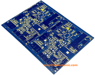
Peelable mask is screen printed by the PCB fabricator, the cost of which can be less than that of an assembly worker adding Kapton tape just before flow soldering.
The use of it is to retain clean PTH holes when a board is sent through a solder bath so that the board can be turned over before components added and sent through the wave soldering machine again.
Some of the masks on the OP example PCB could be joined together so that peeling off is quicker.
It is also recommended to peel it off when the board is still warm, having just come off the solder bath.
This site uses cookies to help personalise content, tailor your experience and to keep you logged in if you register.
By continuing to use this site, you are consenting to our use of cookies.