NigthMoth
Member level 1

Hello all
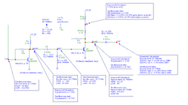
I built and tested a 32.768kHz crystal oscillator circuit based on BJTs in collector feedback bias configuration.
Now I’m trying to understand how it works.
I calculated quiescent voltages for BJTs, some AC parameters and drown equivalent (hope so) model for AC analysis as on pictures below and stucked here.
I'll be very appreciate if someone finds time to check and answer my questions below (sorry if too many).
Question 1:
Does my AC model correct?
Question 2:
Am I correct in understanding that feedback voltage gain is ½ ?
Question 3:
How to calculate Vin1?
Should it be
Vin1 = Vfb*Zin1/(Zout_fb + Rcryst + Zin1) voltage divider calculation?
Question 4:
How to calculate Vin2?
Should it be
Vin2 = Vout1*(Zin2||Xc3)/[(Zin2||Xc3) + Xc2 + Zout1] voltage divider with Xc3 parallel with Zin2?
Question 5:
Where to start analysis?
My guess is:
I should postulate, for example: “Let Vout2 oscillates between 0V and 5.2V”.
Then Vfb oscillates between +2.6V and +5.2V. Taking into account Vfb(quiescent) = 3.26V, it dives -0.66V below and +1.94V above quiescent point.
So AC voltage is -0.66V…+1.94V and I need to feed this AC voltage value into my AC model?
Question 6:
Why there is C2-C3 capacitor voltage divider? I tried to make calculations using formula as in my Question 3, and get Vin2 = 0.035*Vout1 with -60O
phase shift. As I understand, for oscillator one need 360O phase shift, But Q1 and Q2 already provide 180O + 180O shift.
Or C2 and C3 here for other purposes?
Question 7:
According to my calculations, for BJT Collector feedback bias configuration, Vout2 sits at 1.3V and adds 3.9V (up to 5.2Vcc) for High output or drops 1.3V (down to 0V) for low output. So I expect that after C4 (DC blocking capacitor) V(OUT) waveform should altering between +3.9V and -1.3V. But in reality it is between +1.25V and -3.54V.
It looks like test result is mirrored image of my calculations, but I can’t find where I’m wrong (maybe I misunderstood how DC blocking capacitor works?).
Question 8:
What is possible reason I got such a large difference in real and calculated values for Vout1(quiescent) and Vout2(quiescent)?
******
For my analysis I used these formulas and values:
For BJT DC analysis:
Ib = (Vcc - Vbe)/(Rf + hfe*Rc);
Ic = hfe*Ib;
Vout(quiescent) = Vc = Vce = Vcc - Ic*Rc;
For Vfb q-point
Vfb(quiescent) = Ic*Rdown + Vc;
For BJT AC analysis:
re = 26mV/Ic;
ro = 1/hoe = 1/9 uMho = 111k for 2N3904 @IC = 1mA;
Zi = re/(1/hfe + Rc/(Rc+Rf)) (applicable when Rc>>re);
Zo = Rc||Rf (applicable when ro>10*Rc);
Av = -Rc/re (applicable when Rf >> Rc) (“-“ for -180O phase shift);
For crystal + CL
Rcryst ~= Rs*(1+Co/CL)^2 @resonance frequency (from this techical note);
For feedback:
Zo_fb = Rup||(Rdown+Rf);
Av_fb = -Rup/re, or ½ of Av2, so Av_fb = 1/2 is for Vout2;
Values from datasheets:
2N3904 BJT:
- Minimum hfe (@IC = 1mA, Vce = 1V) = 70 (Use it for worst case scenario);
- Vce (@IC = 1mA) = 0.05V;
- Vbe (@IC = 1mA) = 0.7V; [Oscilloscope Q1 = 0.636V, Q2 = 0.636V];
- Rise time (@IC = 1mA) >500 nS (~1uS?);
- Fall time (@IC = 1mA) = 400 nS;
- hoe (@IC = 1mA) ~= 9 uMho;
CFS145 32.768kHz tuning fork crystal:
-Co = 1pF;
-Rs = 40k;
-CL = 12.5p;
I built and tested a 32.768kHz crystal oscillator circuit based on BJTs in collector feedback bias configuration.
Now I’m trying to understand how it works.
I calculated quiescent voltages for BJTs, some AC parameters and drown equivalent (hope so) model for AC analysis as on pictures below and stucked here.
I'll be very appreciate if someone finds time to check and answer my questions below (sorry if too many).
| Circuit: |
| AC model |
| Breadboard |
| Real circuit |
| Output |
Question 1:
Does my AC model correct?
Question 2:
Am I correct in understanding that feedback voltage gain is ½ ?
Question 3:
How to calculate Vin1?
Should it be
Vin1 = Vfb*Zin1/(Zout_fb + Rcryst + Zin1) voltage divider calculation?
Question 4:
How to calculate Vin2?
Should it be
Vin2 = Vout1*(Zin2||Xc3)/[(Zin2||Xc3) + Xc2 + Zout1] voltage divider with Xc3 parallel with Zin2?
Question 5:
Where to start analysis?
My guess is:
I should postulate, for example: “Let Vout2 oscillates between 0V and 5.2V”.
Then Vfb oscillates between +2.6V and +5.2V. Taking into account Vfb(quiescent) = 3.26V, it dives -0.66V below and +1.94V above quiescent point.
So AC voltage is -0.66V…+1.94V and I need to feed this AC voltage value into my AC model?
Question 6:
Why there is C2-C3 capacitor voltage divider? I tried to make calculations using formula as in my Question 3, and get Vin2 = 0.035*Vout1 with -60O
phase shift. As I understand, for oscillator one need 360O phase shift, But Q1 and Q2 already provide 180O + 180O shift.
Or C2 and C3 here for other purposes?
Question 7:
According to my calculations, for BJT Collector feedback bias configuration, Vout2 sits at 1.3V and adds 3.9V (up to 5.2Vcc) for High output or drops 1.3V (down to 0V) for low output. So I expect that after C4 (DC blocking capacitor) V(OUT) waveform should altering between +3.9V and -1.3V. But in reality it is between +1.25V and -3.54V.
It looks like test result is mirrored image of my calculations, but I can’t find where I’m wrong (maybe I misunderstood how DC blocking capacitor works?).
Question 8:
What is possible reason I got such a large difference in real and calculated values for Vout1(quiescent) and Vout2(quiescent)?
******
For my analysis I used these formulas and values:
For BJT DC analysis:
Ib = (Vcc - Vbe)/(Rf + hfe*Rc);
Ic = hfe*Ib;
Vout(quiescent) = Vc = Vce = Vcc - Ic*Rc;
For Vfb q-point
Vfb(quiescent) = Ic*Rdown + Vc;
For BJT AC analysis:
re = 26mV/Ic;
ro = 1/hoe = 1/9 uMho = 111k for 2N3904 @IC = 1mA;
Zi = re/(1/hfe + Rc/(Rc+Rf)) (applicable when Rc>>re);
Zo = Rc||Rf (applicable when ro>10*Rc);
Av = -Rc/re (applicable when Rf >> Rc) (“-“ for -180O phase shift);
For crystal + CL
Rcryst ~= Rs*(1+Co/CL)^2 @resonance frequency (from this techical note);
For feedback:
Zo_fb = Rup||(Rdown+Rf);
Av_fb = -Rup/re, or ½ of Av2, so Av_fb = 1/2 is for Vout2;
Values from datasheets:
2N3904 BJT:
- Minimum hfe (@IC = 1mA, Vce = 1V) = 70 (Use it for worst case scenario);
- Vce (@IC = 1mA) = 0.05V;
- Vbe (@IC = 1mA) = 0.7V; [Oscilloscope Q1 = 0.636V, Q2 = 0.636V];
- Rise time (@IC = 1mA) >500 nS (~1uS?);
- Fall time (@IC = 1mA) = 400 nS;
- hoe (@IC = 1mA) ~= 9 uMho;
CFS145 32.768kHz tuning fork crystal:
-Co = 1pF;
-Rs = 40k;
-CL = 12.5p;