bjihoon
Newbie

I designed conventional TSPC DFF circuit and I aplplied the ideal 4 phase clock(0, 90, 180, 270) to each DFF's clock port like below. (each circuits in the white boxes are same except for input signal.)
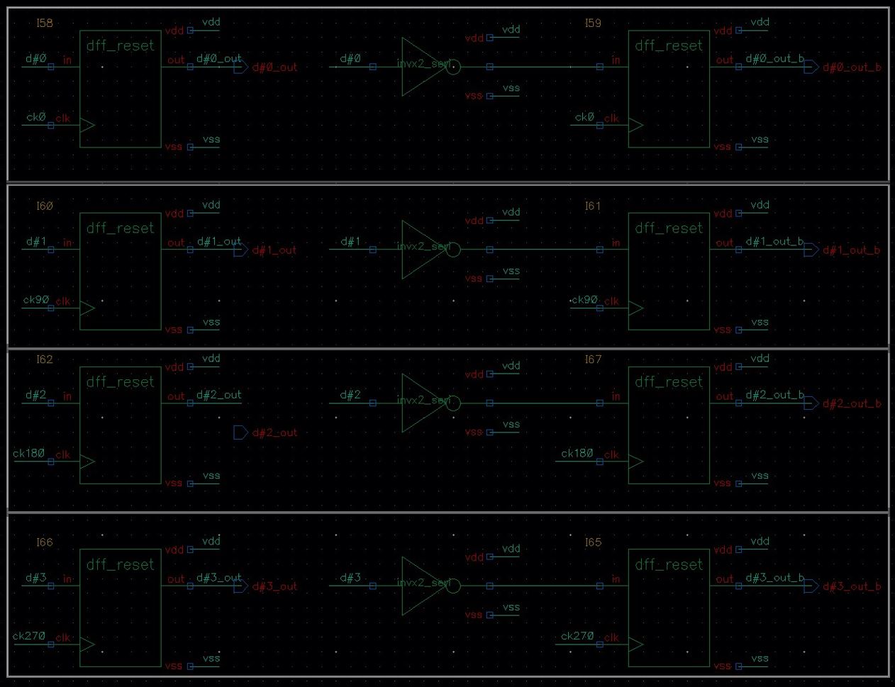
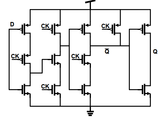 I used this DFF circuit. It is for NRZ to RZ data converting.
And I did post layout simulation. but result is something wrong.
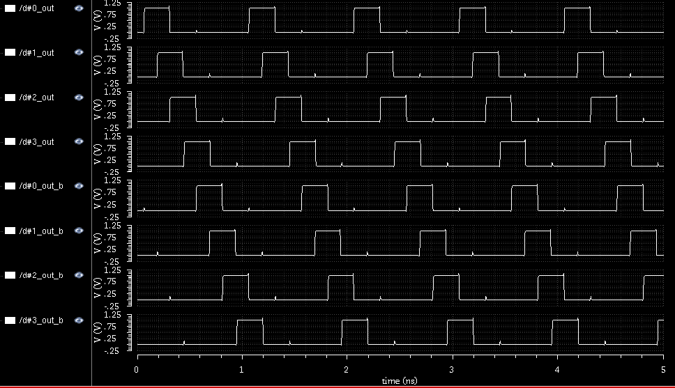
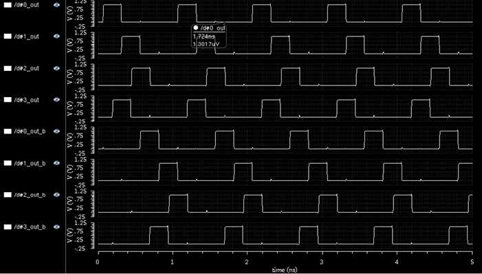
left(above) is schematic simulation and right(below) is post layout simulation. the output was strange.
At first, I thought it's due to parastic cap. So I did everything I could.(using another DFF, changing layout)
But when I used another DFF, the result is almost same.
And I tried one block like below.

In this case, post layout simulation result is almost perfect for each 4 phase clock(0,90,180,270). So I thought it isn't due to parastic cap in layout.
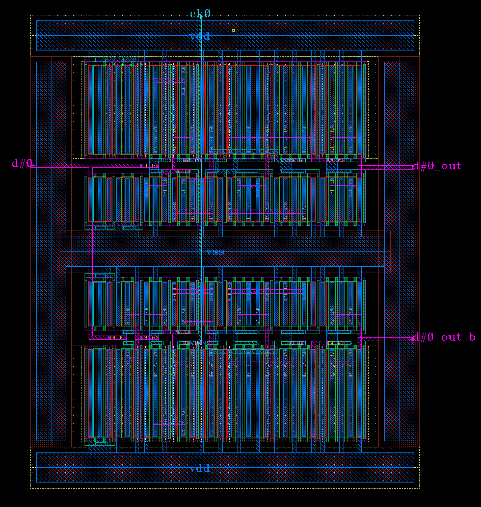
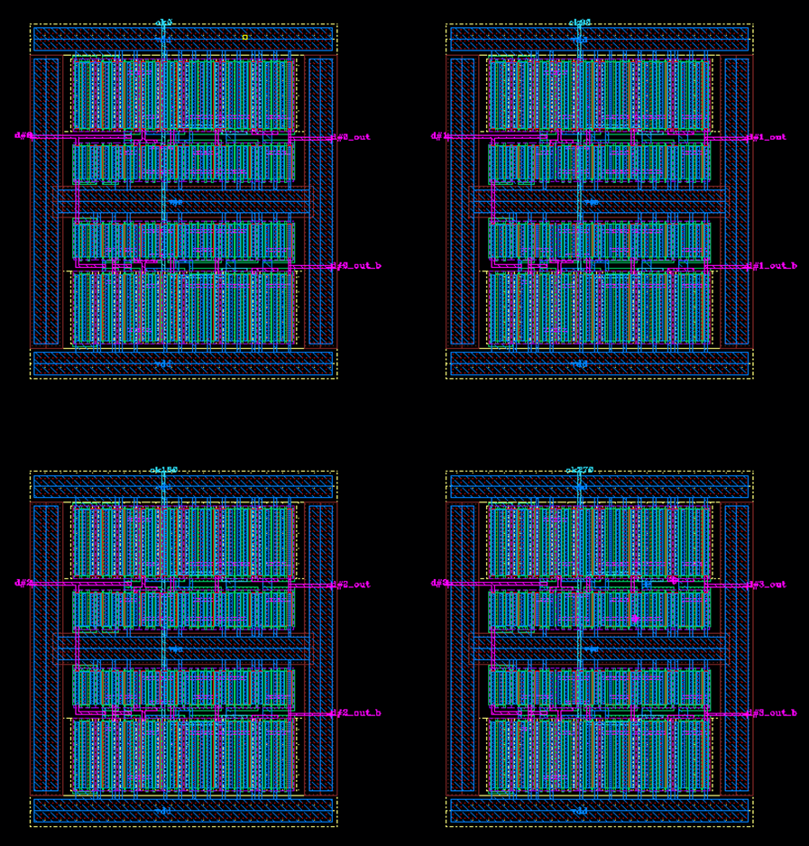
left(above) is one block. And right is total block. In right(below) layout, each block is totally same with left(above) one block. (4 blocks in right have each 4 phase clock.)
In summary, the post layout simulation result was almost perfect when the clock signal was different(0, 90, 180, 270) in one block. But when I simulated in total block, the results were strange.
So I didn't think it is due to parastic cap.
Why does this happen? help me, please.
Additionally, I added a label in layout to see the signal at each point of the circuit. And I did post layout simulation but the results were more strange. I just added the label to layout, but did the result get weird?
please help me. I want to solve this problem. I think this is related to cadence, PEX setting.
And I did post layout simulation. but result is something wrong.
left(above) is schematic simulation and right(below) is post layout simulation. the output was strange.
At first, I thought it's due to parastic cap. So I did everything I could.(using another DFF, changing layout)
But when I used another DFF, the result is almost same.
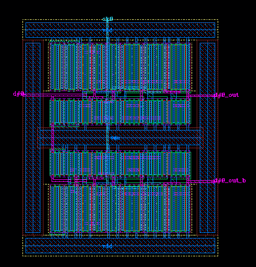
And I tried one block like below.
In this case, post layout simulation result is almost perfect for each 4 phase clock(0,90,180,270). So I thought it isn't due to parastic cap in layout.
left(above) is one block. And right is total block. In right(below) layout, each block is totally same with left(above) one block. (4 blocks in right have each 4 phase clock.)
In summary, the post layout simulation result was almost perfect when the clock signal was different(0, 90, 180, 270) in one block. But when I simulated in total block, the results were strange.
So I didn't think it is due to parastic cap.
Why does this happen? help me, please.
Additionally, I added a label in layout to see the signal at each point of the circuit. And I did post layout simulation but the results were more strange. I just added the label to layout, but did the result get weird?
please help me. I want to solve this problem. I think this is related to cadence, PEX setting.
Last edited:
