mohamis288
Full Member level 3

Hello,
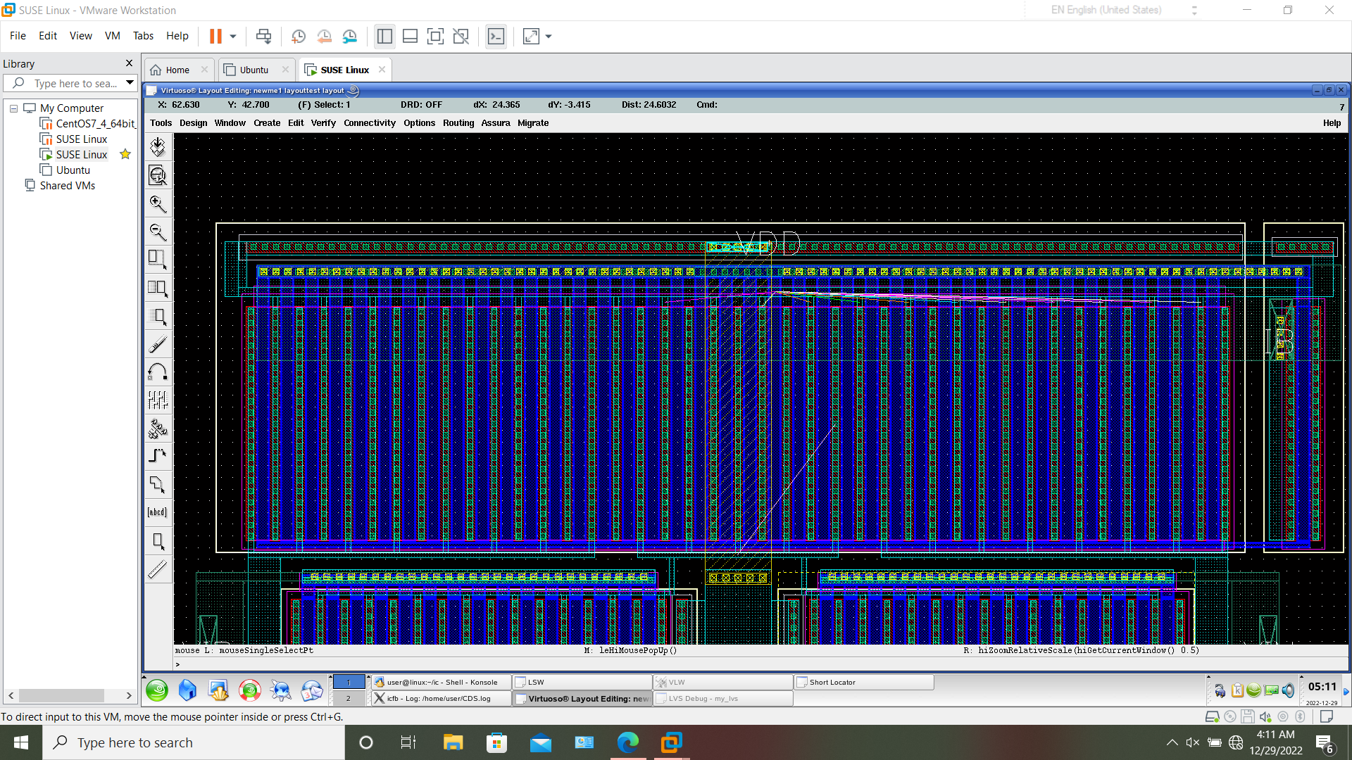
in my layout, I have flattened a single transistor and changed its connections in order to make two transistors from aforementioned transistor. here is the image of this section:

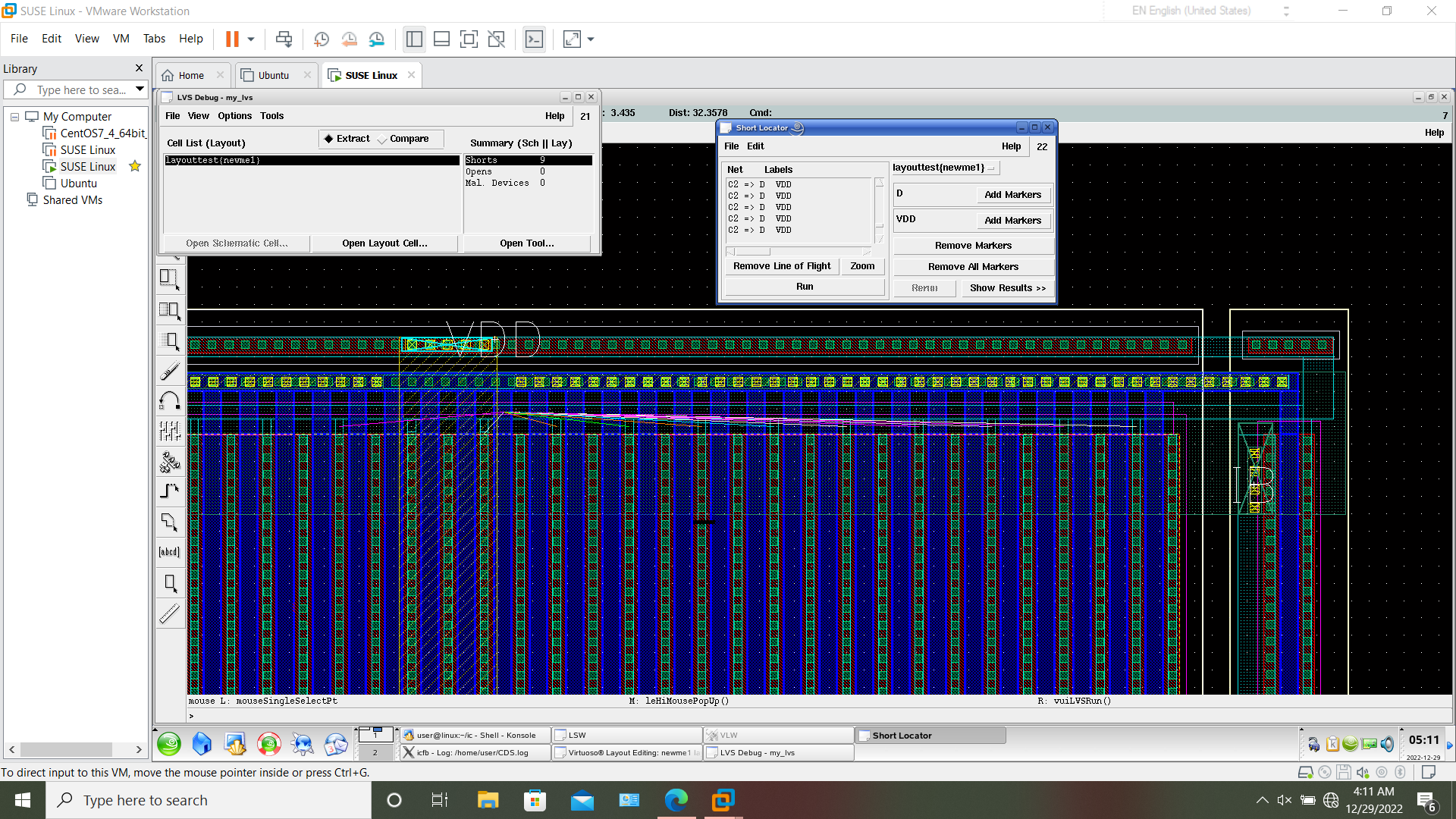
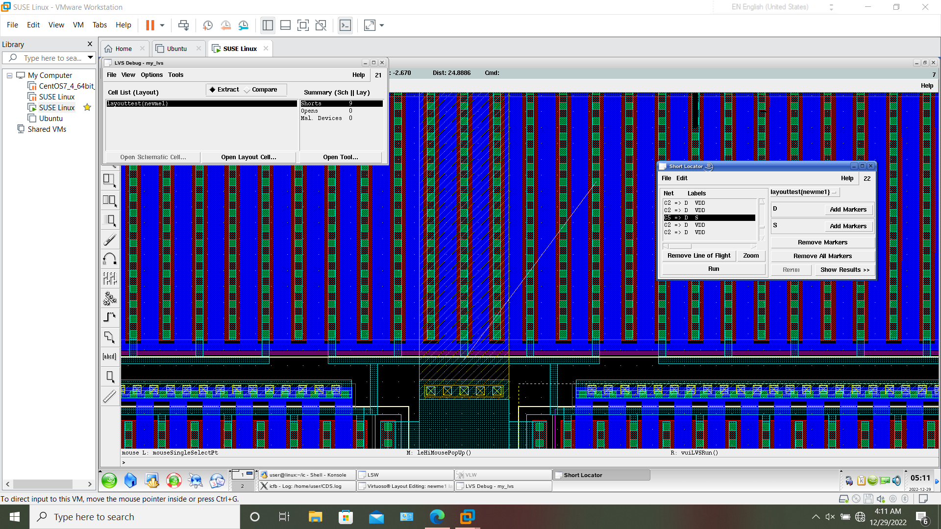
but in LVS window, I receive error related to short-circuited terminals. here this is:


I do want those terminals in image be connected. after analyzing my circuit, I understood that because of flattening mentioned transistor, the order of some source and drain terminals has changed, and also, they have a particular terminal name which are not allowed to be connected to other terminals. because of mentioned reason, three of my PIN in the LVS cannot be matched to schematic. how can I overcome this problem (I hope I am not supposed to change the terminal name of each path one-by-one.)
in my layout, I have flattened a single transistor and changed its connections in order to make two transistors from aforementioned transistor. here is the image of this section:
but in LVS window, I receive error related to short-circuited terminals. here this is:
I do want those terminals in image be connected. after analyzing my circuit, I understood that because of flattening mentioned transistor, the order of some source and drain terminals has changed, and also, they have a particular terminal name which are not allowed to be connected to other terminals. because of mentioned reason, three of my PIN in the LVS cannot be matched to schematic. how can I overcome this problem (I hope I am not supposed to change the terminal name of each path one-by-one.)
