Continue to Site

Welcome to EDAboard.com

Welcome to our site! EDAboard.com is an international Electronics Discussion Forum focused on EDA software, circuits, schematics, books, theory, papers, asic, pld, 8051, DSP, Network, RF, Analog Design, PCB, Service Manuals... and a whole lot more! To participate you need to register. Registration is free. Click here to register now.

Output resistance of current mirror - Simulation Setup

Status
Not open for further replies.

melkord

Full Member level 3
Full Member level 3
Joined
May 18, 2018
Messages
151
Helped
0
Reputation
0
Reaction score
1
Trophy points
18
Activity points
1,772
I usually use small signal formula to calculate output resistance (method 1).
But now want to find a simulation setup to measure it (method 2) so I do not need to input the expression of rout.
A good discussion I found from here and here.

I still do net get the same result between method 1 and method 2.
Could someone give me their correction to my setup?


Result.
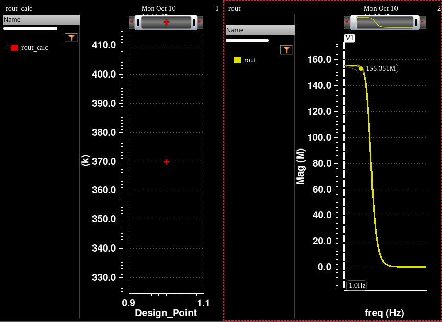
1665411199785.png

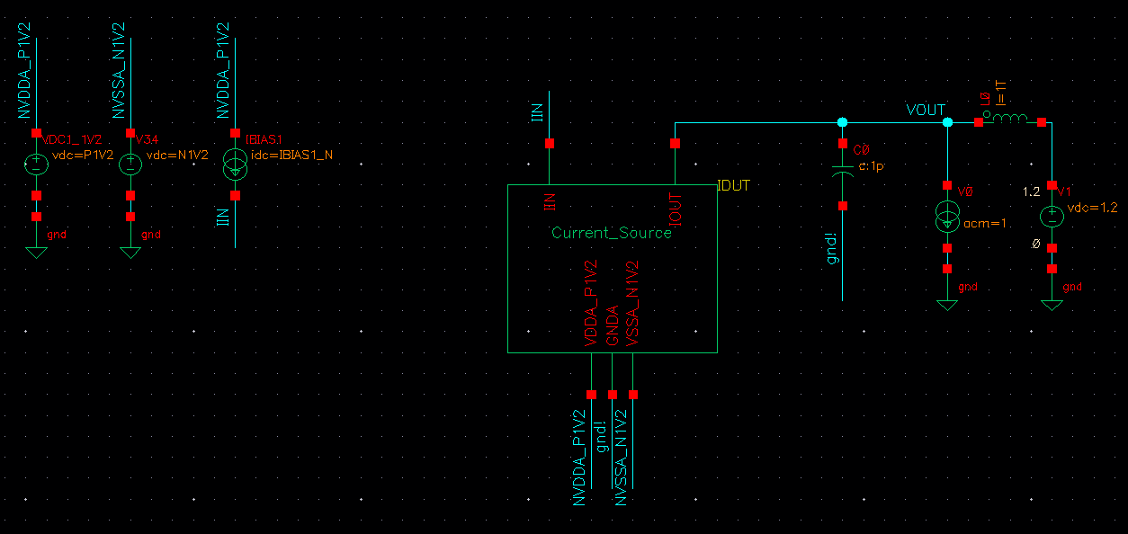
The testbench.
1665411140483.png


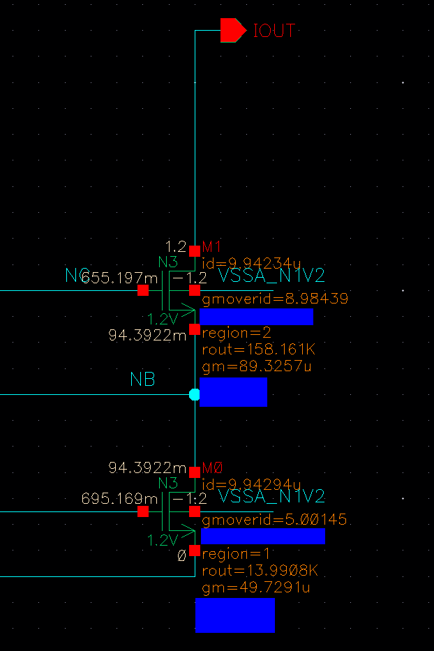
The output transistors.
1665411109083.png
 

M0 is in triode, I suppose that should be fixed first.

Then, are you sure you can use ±1.2V bipolar supplies here? It looks to me like those are 1.2V devices.
M1 Vdb might be way too high at the moment?
 

M0 is in triode, I suppose that should be fixed first.

Then, are you sure you can use ±1.2V bipolar supplies here? It looks to me like those are 1.2V devices.
M1 Vdb might be way too high at the moment?

Here is the simulation result when both transistors are in saturation.
Still I got different results.
1665415798718.png

1665415727448.png
 

And how about the second point?
The bulk is connected to -1.2V, that is not a mistake.
Here is the simulation when VBS of cascode transistor = 0V and VB of bottom transistor = 0V.
Still the results are not the same.
1665417876088.png
1665417831713.png
 

Thanks! The small signal calculation looks reasonable. Not sure what is going on.
Could you try to remove L0, C0 and V0 (the current source), apply an AC stimulus to V1 and re-run the sweep? Then, take 1/i(v1) as your output impedance and compare?
 
Thanks! The small signal calculation looks reasonable. Not sure what is going on.
Could you try to remove L0, C0 and V0 (the current source), apply an AC stimulus to V1 and re-run the sweep? Then, take 1/i(v1) as your output impedance and compare?

Still, they are different.
This setup seems make sense, but I do not understand where I did the mistake.

1665421347129.png


1665421289477.png


1665421263230.png
 

At this point, I also don't understand.
Can you annotate gds? It is worth checking that gds = 1/rout
Also, can you post the full schematic of Current_Source?
Confirmed that gds = 1/rout.
The ideal opamp is from VerilogA.

1665439662265.png


1665439843393.png
 

Oh boy... I hope you're not trolling? The gain of the amplifier improves the output impedance... search for regulated cascode or gain-boosting...

Here I was expecting to see some basic cascode bias stack...
 
Oh boy... I hope you're not trolling? The gain of the amplifier improves the output impedance... search for regulated cascode or gain-boosting...

Here I was expecting to see some basic cascode bias stack...
Ooops..honest mistake. I am not trolling and was not aware that the output impedance was multiplied.
I know regulated cascode for TIA and didnt thought it is the same case here.
I will derive the small signal analysis tomorrow.
Thank you!
 
No worries, glad we cleared it up.
One other thing you could look at is increasing the target Vds and/or the L of the bottom devices.
Right now, the Rout of your cascode is higher than that of the current source itself -- I think that's quite unusual.
 
Status
Not open for further replies.

Part and Inventory Search

Welcome to EDABoard.com

Sponsor

Back
Top