Continue to Site

Welcome to EDAboard.com

Welcome to our site! EDAboard.com is an international Electronics Discussion Forum focused on EDA software, circuits, schematics, books, theory, papers, asic, pld, 8051, DSP, Network, RF, Analog Design, PCB, Service Manuals... and a whole lot more! To participate you need to register. Registration is free. Click here to register now.

[SOLVED] Does GCPW have vias?

Status
Not open for further replies.

x529

Junior Member level 3
Joined
Dec 14, 2019
Messages
30
Helped
0
Reputation
0
Reaction score
0
Trophy points
6
Activity points
265
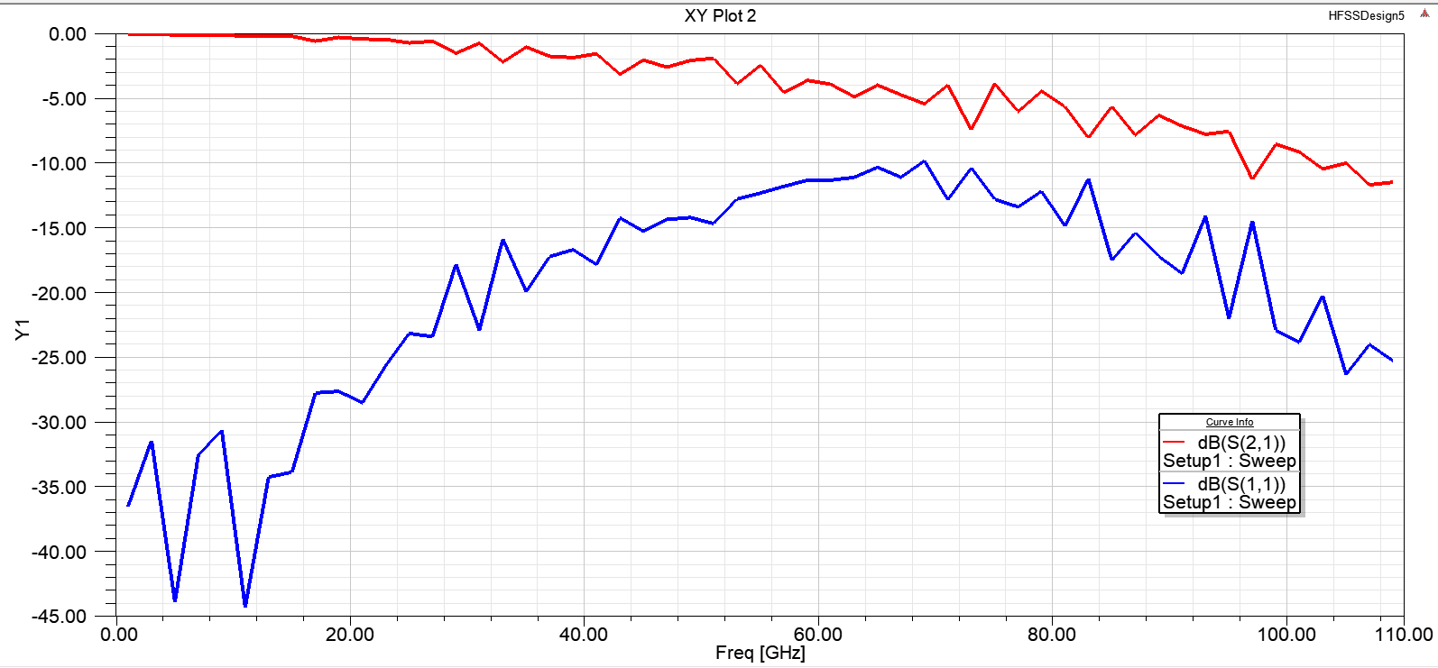
I simulated GCPW, the working frequency band is 1-110GHz, the length is 20mm, and the GCPW loss S21 is very poor; may I make a mistake in my simulation.
Does GCPW have vias? Should the ground on both sides of the upper center conductor be connected to the ground on the lower GND? In the paper, GCPW has no metal pillars.
Thanks.
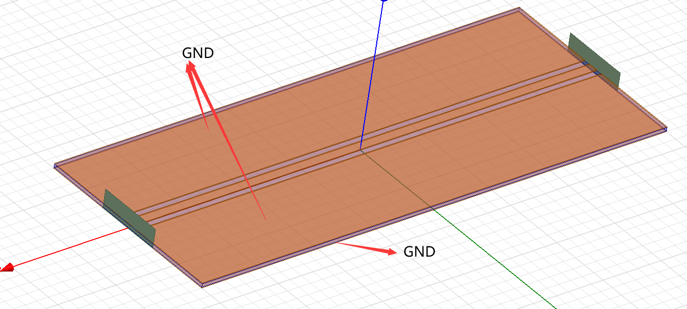
QQ图片20211228114505.png

Figure 1. Structure of GCPW
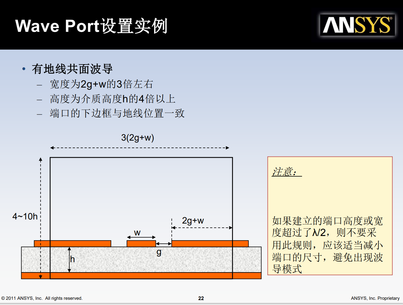
QQ图片20211226214619.png

Figure 2. Wave port settings
QQ图片20211228114501.png

Figure 3. S11 S21
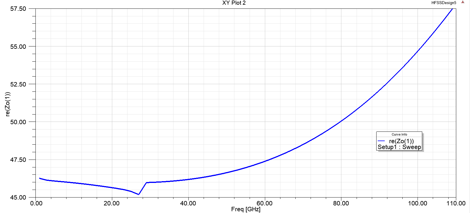
QQ图片20211228114454.png

Figure 4. Port impedance
 

Attachments

  • gcpw.rar
    46.2 KB · Views: 213

Sure, it's Grounded Coplanar Waveguide
There should be vias at both sides of the TL to provide Waveguide effect.
The vias can be placed 1/8 .. 1/16 Lambda pitch space.
 

I agree with BigBoss.

That said, the line in the screenshot looks much too wide for your 110GHz frequency range. If length is 20mm, what is the width?
 

Solution
I agree with BigBoss.

That said, the line in the screenshot looks much too wide for your 110GHz frequency range. If length is 20mm, what is the width?
Thanks for your replay. The total width is 8mm. And I changed the total width(5mm/3mm) to see the simulation results.
--- Updated ---

Sure, it's Grounded Coplanar Waveguide
There should be vias at both sides of the TL to provide Waveguide effect.
The vias can be placed 1/8 .. 1/16 Lambda pitch space.
Thanks for your replay. "The vias can be placed 1/8 .. 1/16 Lambda pitch space." Is the wavelength corresponding to the central frequency(corresponding to 55GHz(DC-110GHz)--- Lumbda= 5.45mm)
--- Updated ---

Sure, it's Grounded Coplanar Waveguide
There should be vias at both sides of the TL to provide Waveguide effect.
The vias can be placed 1/8 .. 1/16 Lambda pitch space.
Through studying the literature, I found that this structure is called CBCPW (Conductor-backed CPW). In the structure of the thesis, the upper surface and the lower surface of GCPW are not connected (without vias), so I mistakenly thought that CBCPW is GCPW.
 

Attachments

  • A1993MK21400024 (1).pdf
    1 MB · Views: 321
Last edited:

I meant width of the center conductor. It looks too wide for 110 GHz.
Please list all dimensions and also the substrate epsilon.

~~~

If you don't connect side grounds to bottom ground, you will observe strange resonances at high frequencies.
 
I meant width of the center conductor. It looks too wide for 110 GHz.
Please list all dimensions and also the substrate epsilon.

~~~

If you don't connect side grounds to bottom ground, you will observe strange resonances at high frequencies.
The width of the center conductor is 0.4mm. I tried a smaller size (0.25mm), and it still observe resonances at high frequencies, the transmission loss is bad.
 

Attachments

  • 9.png
    9.png
    91.8 KB · Views: 261

Place the side grounds (lambda/8 or close at highest frequency) and see what you get.

At the moment you have a 4 conductor system, with different effective epsilon for the top/bottom "ground" conductors.
 

Place the side grounds (lambda/8 or close at highest frequency) and see what you get.

At the moment you have a 4 conductor system, with different effective epsilon for the top/bottom "ground" conductors.
Thank you very much, I got very good transmission performance when add side grounds. And why is the side grounds 1/8 lambda?
 

Sure, it's Grounded Coplanar Waveguide
There should be vias at both sides of the TL to provide Waveguide effect.
The vias can be placed 1/8 .. 1/16 Lambda pitch space.
GCPW (also referred to as conductor-backed CPW, or CB-CPW), does not necessarily need vias, no. As a four conductor system, the waveguide will support 3 (quasi)-TEM modes The usual reason to include the vias is to suppress two of these modes -- a parallel-plate-waveguide-like mode and a parallel-coupled-slot-line-type mode. These modes will parasitically coupler power out of the line to elsewhere in your circuit, and could also radiate, so in traditional PCB applications you don't want them.

The system of conductors with vias will also support waveguide modes as BigBoss has indicated, but of course this mode has inherent upper and lower cutoff frequencies.
 
For some reasons TXLINE calculator from AWR gives about 4.4 ohms difference from your CPW calculator (see the picture). I used Dk, Loss Tangent, and copper thickness of the substrate from your simulation file.
4.4 ohms difference may not be a big deal at 1GHz , but could be at 110GHz.

Also, the ratio of TL length 20mm over substrate thickness 0.127mm, is 157, which is very unusual for a printed line suppose to work at 110GHz.
 

Attachments

  • cpwg.jpg
    cpwg.jpg
    123.6 KB · Views: 230

    x529

    Points: 2
    Helpful Answer Positive Rating
I think the difference is from including metal thickness in calculation. The tool shown above doesn't include metal thickness, as far as I can see.

I used Controlled Impedance Line Designer in ADS, which is solving the 2D EM problem, and get 47 Ohm @ 1GHz and 46.7 Ohm @ 110 GHz for 17µm copper

If we then add via fences on the side, capacitance increases and Zline=sqrt(L'/C') decreases even further. That effect from via fence is NOT included in the 2D cross section calculations!
 

    x529

    Points: 2
    Helpful Answer Positive Rating
I would be cautious about drawing any conclusions about a structure that is modeled over your stated 1-110 GHz frequency band. Just having a correct dielectric constant value over that range is problematic. Various propagation modes are also possible, particularly at the higher end of your bandwidth.

Typically via are used with various "grounded" stripling transmission lines. I am not surprised to see high s21 at higher frequencies. You talk about grounding the center conductor. I take you mean "side grounds" to the "lower" ground so one would end up with a coax like transmission line.

I have found that caution is needed when one excites cpw structures and their various forms. They are mode rich.

This transmission line would not be my first choice for such a wide bandwidth. I would have to look into it carefully to see if it would even be acceptable. I do not have an alternate suggestion, particularly without knowing what your other constraints might be.


My go-to references for this subject are:

Simons, Coplanar Waveguide Circuits, Components, and Systems

Wadell, Transmission Line Design Handbook

Moreno, Microwave Transmission design data

Silver, Microwave Antenna Theory and Design

There is also a wealth of information in the IEEE transactions, particularly APS and MTT among other sources.


Again, my first reaction is that you are trying to accomplish something that is not really practical, Namely a 1 to 110 GHz bandwidth transmission line with some kind of reasonable performance.
 
  • Like
Reactions: x529

    x529

    Points: 2
    Helpful Answer Positive Rating
I think the difference is from including metal thickness in calculation. The tool shown above doesn't include metal thickness, as far as I can see.

I used Controlled Impedance Line Designer in ADS, which is solving the 2D EM problem, and get 47 Ohm @ 1GHz and 46.7 Ohm @ 110 GHz for 17µm copper

If we then add via fences on the side, capacitance increases and Zline=sqrt(L'/C') decreases even further. That effect from via fence is NOT included in the 2D cross section calculations!
Thanks! I agree with you. The impedance calculator is not include the vias metal wall.
--- Updated ---

I would be cautious about drawing any conclusions about a structure that is modeled over your stated 1-110 GHz frequency band. Just having a correct dielectric constant value over that range is problematic. Various propagation modes are also possible, particularly at the higher end of your bandwidth.

Typically via are used with various "grounded" stripling transmission lines. I am not surprised to see high s21 at higher frequencies. You talk about grounding the center conductor. I take you mean "side grounds" to the "lower" ground so one would end up with a coax like transmission line.

I have found that caution is needed when one excites cpw structures and their various forms. They are mode rich.

This transmission line would not be my first choice for such a wide bandwidth. I would have to look into it carefully to see if it would even be acceptable. I do not have an alternate suggestion, particularly without knowing what your other constraints might be.


My go-to references for this subject are:

Simons, Coplanar Waveguide Circuits, Components, and Systems

Wadell, Transmission Line Design Handbook

Moreno, Microwave Transmission design data

Silver, Microwave Antenna Theory and Design

There is also a wealth of information in the IEEE transactions, particularly APS and MTT among other sources.


Again, my first reaction is that you are trying to accomplish something that is not really practical, Namely a 1 to 110 GHz bandwidth transmission line with some kind of reasonable performance.
Thanks for your reply. It's my pleasure to communicate with you.
Yes, I am trying to design broadband transmission line (Frequency: DC- 110GHz). If the TL has the advantages of broadband, low loss and low transmission line. However, I think that it is a meaningful things. Here are the reasons:
With the rapid development of electronics and integrated circuit technology, high-speed digital circuit interconnection transmission, picosecond interconnection, and chip interconnection have great development potential. The design of high-speed systems must face signal integrity issues such as interconnect delay, reflection, crosstalk, and transmission line effects. System-on-chip, integrated system, and module interconnection all require low latency and low dispersion to maintain signal integrity. Ultra-wideband communication technology does not need to use a carrier wave, but transmits and receives extremely narrow pulses to achieve data transmission, which has a bandwidth of the order of GHz. We designed a DC-110GHz ultra-wideband transmission line to meet this high-speed demand.
As a graduate student, I'm not sure if this is true.

I look forward to your criticism and correction if there are any shortcomings.
 
Last edited:

Hello x529,

Do you have a transmission line "specification" in mind? Do you have values to place on the conventional characteristics: s11, s21, Zo? How about size and materials? PCB looks like the medium you are considering but maybe you have something else in mind? You mention UWB applications. That would add an additional wrinkle of dispersion of the pulses; group velocity and group velocity variation issues; and possible inter-signal interference issues.

How are you going to insert and extract the signals into your transmission line? Are you planning on building hardware? Test fixtures? Is this going to be a project in analysis or modeling? At 100 GHz manufacturing tolerances will present a particular challenge compared to what is faced at 1 GHz.

On the subject of vias: The are often present to provide DC continuity for collateral components. A row of vias can be convenient were DC ground connections are needed throughout some PCB structure. They can also be used for transmission mode controls or to suppress undesired radiation either into space or within a PCB structure. My first concern is how a via array might appear at 100 GHz compared to 1 GHz. Anything discrete would be a particular challenge over your bandwidth.

I am back to a very basic question, are you trying to pick apart GCPW transmission lines in particular or are you trying to find a structure suitable for 1 GHz to 100 GHz?
Hello Azulykit,
Thanks for your reply. It's my pleasure to communicate with you.
I think the transmission line should have low loss, broadband performance. And this is also my PhD thesis, though I think it is hard for me to deaign a new low loss, broadband TL. I am trying to design a new TL from DC to 110GHz, however this work has not completed now. It hasn't been fabricated and measured now. I will do it in the fruture.
Through simulation reaults(S11,S21), I am trying to compare with the GCPW, CPW, SIW, Microstrip line transmission lines to show excellent performance.
In my design, I would consider dispersion, loss, bandwidth and S parameters like you said.


Status
Not open for further replies.

Part and Inventory Search

Welcome to EDABoard.com

Sponsor

Back
Top