Continue to Site

Welcome to EDAboard.com

Welcome to our site! EDAboard.com is an international Electronics Discussion Forum focused on EDA software, circuits, schematics, books, theory, papers, asic, pld, 8051, DSP, Network, RF, Analog Design, PCB, Service Manuals... and a whole lot more! To participate you need to register. Registration is free. Click here to register now.

[SOLVED] using Enable decoder and AND gates to switch between two function

Status
Not open for further replies.

MSAKARIM

Full Member level 3
Full Member level 3
Joined
Jun 2, 2015
Messages
154
Helped
1
Reputation
2
Reaction score
4
Trophy points
1,298
Visit site
Activity points
2,528
I have two functions that work with the same input data as shown in the figure. They aren't needed at the same time, so I need to clock only the required function to save calculations and power by the not used one. I used a decoder with AND gates to create sub-clocks for each function. Is this method effective in hardware implementation ? is my thought is right?
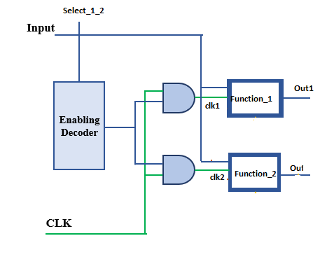
22.PNG
 

gating clocks is not recommended for FPGAs especially for fast fmax.
You can use reset instead to stop logic except clock.
 
gating clocks is not recommended for FPGAs especially for fast fmax.
You can use reset instead to stop logic except clock.
Do you mean using the same concept of decoder and AND gates but in this case to reset the unrequired functions instead of clocking the required?
 

Yes keep it in reset. this will stop logic but not clock. Alternatively use clock enable on every register.
Gating clock leads to hold violations even at low speeds. Though you can try it if it passes timing.
 
Yes keep it in reset. this will stop logic but not clock. Alternatively use clock enable on every register.
Gating clock leads to hold violations even at low speeds. Though you can try it if it passes timing.
Yes keep it in reset. this will stop logic but not clock >> this will save power too, right?
 

power due logic signals toggling will be saved but that of clock itself will stay as clock is running freely nonstop.
 

It could be ASIC terminology as they love intelligent stuff.
The best in terms of power is to switch off clock completely. If you want to go that way then for FPGA you have to use two PLLs or any vendor clock gating module if available.
 

    MSAKARIM

    Points: 2
    Helpful Answer Positive Rating
Hi,

I'm not a specialst here. Maybe a specialist can review my idea.

If I'm not mistaken then there are two major sources of signal switching current in CMOS circuits.
* the capacitance of the traces
* the gates switching

If this is the case then on FPGAs the clock gating idea does not work as expected.
Usually the clock is spread all over the chip, hard wired, so that every gate has access to it.
So clock gating won't reduce the clock wiring capacitance.
Then there are the switching gates.
I use clock_enable to avoid gates from switching.Don't know whether reset makes a difference.

If all this is true, then a gated clock does not significantly reduce current (compaired to clock_enable) but may increase wiring capacitance (when clock enabled) because now the gated clock needs additionally to be wired to all the gates which use it.

I'd be interested in real part current measurements of both solutions.

Klaus
 

    MSAKARIM

    Points: 2
    Helpful Answer Positive Rating
The circuit shown on post #1 surely is not what you wanted to do, once the same clock is AND'ed from decoder at both clock Functions 1,2. BTW, even the synchronous reset approach should not be suited. Perhaps it is worthy to have a look at implementations of "Clock multiplexer for glitch-free clock".
this concept "Clock multiplexer for glitch-free clock" is suitable for two sources of clocks and I want to mux between them isn't it?
in my question, I have only one clock source and I want to time multiplex it for the two functions, ex. I want function_1 only to see the clock when I select that and vice-versa.
 

Hi,

Let´s imagin the SELECT signal of post#1 comes form a clocked logic or FF.
So it is synchronous. So far so good.

Now let´s imagine the SELECT signal is generated/synchronized with the rising clock edge.
Then the SELECT signal is a bit delayed to the clock edge.

Now if you AND the clock and the SELECT signal (disabling = falling): The rising clock signal comes first then the SELECT signal goes LOW a little later.
The output goes HIGH with the rising clock edge (at this time the clock was still eanbled) but a very short time late it gets disabled and goes LOW. This is called a "glitch".

Since it is a very short pulse it may cause your function toe
* see a true clock pulse
* not to see a clock pulse
* or sometimes see a clock pulse
--> unreliable function.

(Sadly I don´t have a good drawing tool at my tablet)

But as already recommended: do a real test or do a simulation.

Klaus
 
in my question, I have only one clock source and I want to time multiplex it for the two functions
What about using the above proposed "Clock multiplexer for glitch-free clock" circuit with the same clock, but without the OR logic at the end; in other words, only the FF circuitry itself ? This way, the output at the AND become the selected clock. Note that the FF's inbetween is what ensures the non-occurrence of glitches when selecting one of both clock outputs.
 
Hi,

GCLK, RCLK, PLL_OUT seem to be dedicated clock nets ... that can be enabled/disabled. I guess these are not usual signal paths. It may be a hardware option by the Cyclone devices, not every FPGA will have them.

Also note that the enable D-FF uses inverting clock with respect to AND input to avoid glitches.

Klaus
 
Hi Andre_teprom,

I see your focus is on the clocks cross-over but your circuit is otherwise close to original posted diagram which did not specify how decoding was implemented.

Unlike ASICs, FPGAs are very sensitive to clock gating. I never do it. The thing that I stressed on was to do with clock gating which leads to hold violations unless the clocks are reconnected to global net and the device supports such clock enable.
 
Thanks for all the comments and this useful discussion, but now I'm confused because I'm going to implement this model using VHDL
I will use Xilinx Virtex7 FPGA,
I tried solutions of @andre_teprom and @kaz1 in simulation, they worked well.
I want to make a global solution of clock gating without glitches in FPGA ( I will write it in VHDL).
what one of them is the best? both ? or should I see how Virtex 7 implement the clock gating ?
--- Updated ---

Hi,

Let´s imagin the SELECT signal of post#1 comes form a clocked logic or FF.
So it is synchronous. So far so good.

Now let´s imagine the SELECT signal is generated/synchronized with the rising clock edge.
Then the SELECT signal is a bit delayed to the clock edge.

Now if you AND the clock and the SELECT signal (disabling = falling): The rising clock signal comes first then the SELECT signal goes LOW a little later.
The output goes HIGH with the rising clock edge (at this time the clock was still eanbled) but a very short time late it gets disabled and goes LOW. This is called a "glitch".

Since it is a very short pulse it may cause your function toe
* see a true clock pulse
* not to see a clock pulse
* or sometimes see a clock pulse
--> unreliable function.

(Sadly I don´t have a good drawing tool at my tablet)

But as already recommended: do a real test or do a simulation.

Klaus
I did a simulation and it worked well (No glitches), is there possibles that it works well in simulation but not in real-time?
--- Updated ---

Thanks for all the comments and this useful discussion, but now I'm confused because I'm going to implement this model using VHDL
I will use Xilinx Virtex7 FPGA,
I tried solutions of @andre_teprom and @kaz1 in simulation, they worked well.
I want to make a global solution of clock gating without glitches in FPGA ( I will write it in VHDL).
what one of them is the best? both ? or should I see how Virtex 7 implement the clock gating ?
--- Updated ---


I did a simulation and it worked well (No glitches), is there possibles that it works well in simulation but not in real-time?
If I use this "https://www.fpgadeveloper.com/2011/09/code-templates-clock-mux.html/" after the Decoder and gates (consider clk1,clk2) it will work well?
 
Last edited:

Simulation needs to be timing based(not just functional) to check the clock design.
I suggest once you gate the clocks in whatever way make sure the two output clocks are then reconnected to global net. I expect there are settings in compiler for that.

However for a given build if it passes timing (setup & hold) then you are ok.
 
I did a simulation and it worked well (No glitches), is there possibles that it works well in simulation but not in real-time?
--- Updated ---
HDL simulations don't show setup/hold/pulse_width violations, so in the real-world the design might not work as expected.

The real world design depends on the placement and routing of the FPGA post implementation. The only way to check is to run both corners on the back annotated netlist of the implemented design (which you will have to do every time you rebuild the design)
 
Status
Not open for further replies.

Part and Inventory Search

Welcome to EDABoard.com

Sponsor

Back
Top