Continue to Site

Welcome to EDAboard.com

Welcome to our site! EDAboard.com is an international Electronics Discussion Forum focused on EDA software, circuits, schematics, books, theory, papers, asic, pld, 8051, DSP, Network, RF, Analog Design, PCB, Service Manuals... and a whole lot more! To participate you need to register. Registration is free. Click here to register now.

Subthreshold Two Stage Op-Amp Vbias (V_REF1 & V_REF2)

Status
Not open for further replies.

Desmonday

Newbie level 6
Newbie level 6
Joined
May 7, 2021
Messages
11
Helped
0
Reputation
0
Reaction score
2
Trophy points
3
Activity points
142

Attachments

  • Untitled.png
    Untitled.png
    29 KB · Views: 245
  • Untitled.png
    Untitled.png
    29 KB · Views: 185

Hi,

The text says:
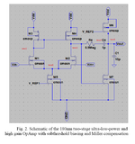
Once appropriate aspect ratios were
determined for all the MOSFETs, the DC bias voltage VREF1
was set based on the gain considerations after performing a DC
analysis on the first stage
of the op-amp. VREF2 was
subsequently set to meet the desired gain of the overall
amplifier.
I guess you or better say your application decides the gain requirement.

Klaus
 
Hi,

The text says:

I guess you or better say your application decides the gain requirement.

Klaus
Hello KlausST, I appreciate your answer. Where should I connect the V_Ref2 and V_Ref1? Should I bias both of the terminals? Or should I connect it to Vdd and Gnd respectively?
 

Hi,

The text says
* you need to consider the (required) gain. (We can not know this)
* you need to do a DC analysis.(it makes no sense that anybody else than you does the DC analysis)
Then you will find out Ref voltage.

I guess it is somewhere inbetween GND and VCC.

An experienced IC designer may give you more detailed informations.

Klaus
 
Those FETs are used as current sources as I see (M5: diff pair. tail current source, M6: active load of 2nd stage).

So don't connect VREF1,2 to supply rails, M5,6 won't saturate, they going to operate as small resistors.
Connect them to diode connected FET-s rather.

The diode connected devices will generate bias voltages for the M5,M6 current sources (=Vgs,Vsg) if you connect a constant current to the diode connected device.
--- Updated ---

And if you want to save some time and pain connect M7 gate to VREF1 and M6 gate to output of the 1st stage.

To keep M7 in saturation a relatively low potential should be on its gate, M6 need a potential closer to VDD for the same reason.

About biasing, CMOS OPAMPs you can learn a lot from Behzad Razavi's book, Design of CMOS analog integrated circuits. Good luck!
 
Last edited:
The circuit you attached has nothing directly to do with it being biased in subthreshold. It is probably the most common type of two stage amplifier out there with Miller compensation.

If being used in subthreshold the size and bias of the transistors is what matters and that isn't given.

I suggest looking, as frankrose suggested, in Behzad Razavis book for reference. And if you search some more you will find papers where more detail is given for the circuit which might give you some more insight.

Also think about why you want it in subthreshold. Do you need lower power? Lower supply voltage? A lot of performance parameters gets a hit when an amplifier is biased in subthreshold. Some might not be obvious at a first glance such as matching.

Since you say it will be used in a bandgap and you might not have a current reference, read up on constant-gm circuits.
 

Status
Not open for further replies.

Part and Inventory Search

Welcome to EDABoard.com

Sponsor

Back
Top