Continue to Site

Welcome to EDAboard.com

Welcome to our site! EDAboard.com is an international Electronics Discussion Forum focused on EDA software, circuits, schematics, books, theory, papers, asic, pld, 8051, DSP, Network, RF, Analog Design, PCB, Service Manuals... and a whole lot more! To participate you need to register. Registration is free. Click here to register now.

SRAM Controller using IPCore "AXI EMC 3.0" on Xilinx FPGA board

Status
Not open for further replies.

FlyingDutch

Advanced Member level 1
Joined
Dec 16, 2017
Messages
458
Helped
45
Reputation
92
Reaction score
55
Trophy points
28
Location
Bydgoszcz - Poland
Activity points
5,027
Hello,

some time ago I described my struggling with implementatuion for very simple "SRAM controller" - see this link:

https://www.edaboard.com/threads/issue-with-port-buffering-inout-spartan7-board.395904/

After long time this struggle ended with success - this simple controller was working. The issue is that implementation had very bad performance and wasn't suitable for using in real project (for my needs only). It was the reason that I have started looking for better implementation of SRAM controller. I noticed that in "Xilinx Vivado" is available fre IPCore called "AXI EMC v.3.0" (this is shortcut for: AXI External Memory Controller) - see this link:

https://www.xilinx.com/support/documentation/ip_documentation/axi_emc/v3_0/pg100-axi-emc.pdf

I tried in Vivado project to fulfill all parameters for my memory IC (CY7C1041DV33) - see screenshot:
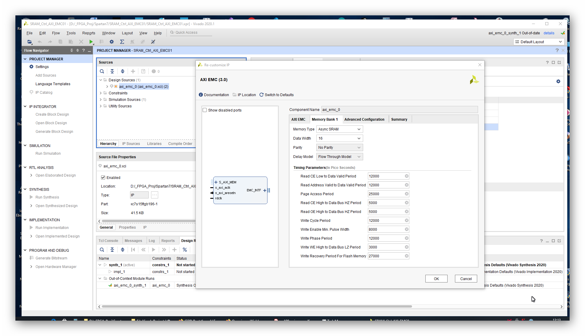
--- Updated ---

AXI_EMC_01.png

The problem is that this IPCore interface is very complicated - both AXI part end SRAM IC. Here is generated for this IP Core VHDL entity port:


Code:
ENTITY axi_emc_0 IS

  PORT (
    s_axi_aclk : IN STD_LOGIC;
    s_axi_aresetn : IN STD_LOGIC;
    rdclk : IN STD_LOGIC;
    s_axi_mem_awid : IN STD_LOGIC_VECTOR(3 DOWNTO 0);
    s_axi_mem_awaddr : IN STD_LOGIC_VECTOR(31 DOWNTO 0);
    s_axi_mem_awlen : IN STD_LOGIC_VECTOR(7 DOWNTO 0);
    s_axi_mem_awsize : IN STD_LOGIC_VECTOR(2 DOWNTO 0);
    s_axi_mem_awburst : IN STD_LOGIC_VECTOR(1 DOWNTO 0);
    s_axi_mem_awlock : IN STD_LOGIC;
    s_axi_mem_awcache : IN STD_LOGIC_VECTOR(3 DOWNTO 0);
    s_axi_mem_awprot : IN STD_LOGIC_VECTOR(2 DOWNTO 0);
    s_axi_mem_awvalid : IN STD_LOGIC;
    s_axi_mem_awready : OUT STD_LOGIC;
    s_axi_mem_wdata : IN STD_LOGIC_VECTOR(31 DOWNTO 0);
    s_axi_mem_wstrb : IN STD_LOGIC_VECTOR(3 DOWNTO 0);
    s_axi_mem_wlast : IN STD_LOGIC;
    s_axi_mem_wvalid : IN STD_LOGIC;
    s_axi_mem_wready : OUT STD_LOGIC;
    s_axi_mem_bid : OUT STD_LOGIC_VECTOR(3 DOWNTO 0);
    s_axi_mem_bresp : OUT STD_LOGIC_VECTOR(1 DOWNTO 0);
    s_axi_mem_bvalid : OUT STD_LOGIC;
    s_axi_mem_bready : IN STD_LOGIC;
    s_axi_mem_arid : IN STD_LOGIC_VECTOR(3 DOWNTO 0);
    s_axi_mem_araddr : IN STD_LOGIC_VECTOR(31 DOWNTO 0);
    s_axi_mem_arlen : IN STD_LOGIC_VECTOR(7 DOWNTO 0);
    s_axi_mem_arsize : IN STD_LOGIC_VECTOR(2 DOWNTO 0);
    s_axi_mem_arburst : IN STD_LOGIC_VECTOR(1 DOWNTO 0);
    s_axi_mem_arlock : IN STD_LOGIC;
    s_axi_mem_arcache : IN STD_LOGIC_VECTOR(3 DOWNTO 0);
    s_axi_mem_arprot : IN STD_LOGIC_VECTOR(2 DOWNTO 0);
    s_axi_mem_arvalid : IN STD_LOGIC;
    s_axi_mem_arready : OUT STD_LOGIC;
    s_axi_mem_rid : OUT STD_LOGIC_VECTOR(3 DOWNTO 0);
    s_axi_mem_rdata : OUT STD_LOGIC_VECTOR(31 DOWNTO 0);
    s_axi_mem_rresp : OUT STD_LOGIC_VECTOR(1 DOWNTO 0);
    s_axi_mem_rlast : OUT STD_LOGIC;
    s_axi_mem_rvalid : OUT STD_LOGIC;
    s_axi_mem_rready : IN STD_LOGIC;
    mem_dq_i : IN STD_LOGIC_VECTOR(15 DOWNTO 0);
    mem_dq_o : OUT STD_LOGIC_VECTOR(15 DOWNTO 0);
    mem_dq_t : OUT STD_LOGIC_VECTOR(15 DOWNTO 0);
    mem_a : OUT STD_LOGIC_VECTOR(31 DOWNTO 0);
    mem_ce : OUT STD_LOGIC_VECTOR(0 DOWNTO 0);
    mem_cen : OUT STD_LOGIC_VECTOR(0 DOWNTO 0);
    mem_oen : OUT STD_LOGIC_VECTOR(0 DOWNTO 0);
    mem_wen : OUT STD_LOGIC;
    mem_ben : OUT STD_LOGIC_VECTOR(1 DOWNTO 0);
    mem_qwen : OUT STD_LOGIC_VECTOR(1 DOWNTO 0);
    mem_rpn : OUT STD_LOGIC;
    mem_adv_ldn : OUT STD_LOGIC;
    mem_lbon : OUT STD_LOGIC;
    mem_cken : OUT STD_LOGIC;
    mem_rnw : OUT STD_LOGIC;
    mem_cre : OUT STD_LOGIC;
    mem_wait : IN STD_LOGIC_VECTOR(0 DOWNTO 0)
  );

END axi_emc_0;


I am aware that next step should be adding to project Soft-Processor (for example Xilinx Microblaze ) which is able to send data to SRAM memory over AXI BUS. I was looking for such example oprojects but this serch was unsuccessful. Could somebody share with me example project wich is using "AXI EMC" (best with Microblaze). But if someone has example code using "AXI EMC" without soft-processor I am aslo interested in it. Any hints to implementing such SRAM controller are warmly welcome.


Thanks in advance and Regards
 

Hello,

in the context of my post I would like to ask if "Wishbone Bus" is still in common use or it had been replaced by AXI Bus?
I am asking because for example "Instant SoC" is using Wisbone Bus (and "Instant SoC" is very simple to implementation) and I can use it for SRAM connection.
IpCore "AXI EMC" is using AXI Bus and for connection SRAM I have to use much more complicated "Microblaze" SoftCPU.

Best Regards
 

I don't know what is Instant SoC.
Wishbone Bus is rarely used now-a-days. I have seen them only in some freely available to use legacy IP cores. For Xilinx FPGAs AMBA protocols is certainly the de-facto standard.
In my opinion if you are developing an IP core, then using the Wishbone within the design should be ok. In other words if the Wishbone bus is buried deep inside the design and is functioning correctly then no problem. I would object to the use of Wishbone Bus at the interface because when interfacing this core, someone might have to write/buy extra wrapper logic (since Wishbone is not common).
 
Hello,

"InstantSoC" is project where you write code in C language - you make instances of MCU peripherals (for example GPIO, UART, timer, Wishbone bus) and build project. There is under C compiler generator wich is generating VHDL code of RISC-V( MCU with peripherals. Very quick and it is working OK. Here is link to it's website:

https://www.fpga-cores.com/instant-soc/

and class index (generated by Oxygen):

https://www.fpga-cores.com/ISOCCL/html/annotated.html

Best Regards
 

I noticed that in "Xilinx Vivado" is available fre IPCore called "AXI EMC v.3.0" (this is shortcut for: AXI External Memory Controller) - see this link:
....
The problem is that this IPCore interface is very complicated - both AXI part end SRAM IC.
....
I am aware that next step should be adding to project Soft-Processor (for example Xilinx Microblaze ) which is able to send data to SRAM memory over AXI BUS. I was looking for such example oprojects but this serch was unsuccessful. Could somebody share with me example project wich is using "AXI EMC" (best with Microblaze). But if someone has example code using "AXI EMC" without soft-processor I am aslo interested in it. Any hints to implementing such SRAM controller are warmly welcome.
If you are trying to implement the design by instantiating the VHDL directly into another VHDL file then you aren't building your SoC design in Vivado using the standard methodology.

SoC designs in Vivado are meant to be done using their block design tool, which avoids having to understand or determine how to connect the "complicated" AXI bus.

There are examples of Vivado block designs that have a variety of peripherals that are on Xilinx's support site. There might not be ones specific to the Spartan 7 but you can look at the ones for the Zynq and see how those BDs are done to build one for the Spartan 7.
Hello @ads-ee,

Thanks for your answer. Yes I know how it looks for Zynq or Microblaze, but I don't like this block design in Vivado (it is not very readable for me). So I decided to use "Instant SoC" with Wisbone bus and IpCore "ZBT SRAM Controller" which has also Wisbone Bus. Here is link how to implement "Instant SoC" with Wisbone Bus:

https://www.fpga-cores.com/wishbone/

, and here is link to "ZBT SRAM Controller" on Opencores.org website:

https://opencores.org/projects/zbt_sram_controller

Here is interface to "ZBT SRAM Controller" - ports of its entity:

Code:
-- WB: MASTER MUST NOT insert wait states!
-- WB: maximum burst length is 4 (but bursts may follow without wait states in between)

entity zbt_top is
    Port (  clk : in STD_LOGIC;
            reset : in STD_LOGIC;

            SRAM_CLK : out STD_LOGIC; --Synchronous Clock (up to 200 MHz)

            --A burst mode pin (MODE) defines the order of the burst sequence. When tied HIGH, the interleaved burst sequence is selected.
            --When tied LOW, the linear burst sequence is selected.
            SRAM_MODE : out STD_LOGIC; --Burst Sequence Selection (pulled down on PCB)
            
            SRAM_CS_B : out STD_LOGIC; --Synchronous Chip Enable (CE\, pulled up on PCB)
            
            --For write cycles following read cycles, the output buffers must be disabled with OE\, otherwise data bus contention will occur
            SRAM_OE_B : out STD_LOGIC; --Output Enable (OE\, pulled up on PCB)
            
            --Write cycles are internally self-timed and are initiated by the rising edge of the clock inputs and when WE\ is LOW.
            SRAM_FLASH_WE_B : out STD_LOGIC; --Synchronous Read/Write Control Input (pulled up on PCB)
            
            --All Read, Write and Deselect cycles are initiated by the ADV input. When the ADV input is HIGH the internal
            --burst counter is incremented. New external addresses can be loaded when ADV is LOW.
            SRAM_ADV_LD_B : out STD_LOGIC; --Synchronous Burst Address Advance/Load (pulled down on PCB)


            SRAM_BW0 : out STD_LOGIC; --Synchronous Byte Write Enable 0 (active low)
            SRAM_BW1 : out STD_LOGIC; --Synchronous Byte Write Enable 1 (active low)
            SRAM_BW2 : out STD_LOGIC; --Synchronous Byte Write Enable 2 (active low)
            SRAM_BW3 : out STD_LOGIC; --Synchronous Byte Write Enable 3 (active low)
            
            --SRAM_FLASH_A0 : out STD_LOGIC; --not connected to SRAM!
            SRAM_FLASH_A1 : out STD_LOGIC; --Synchronous Address Input 0
            SRAM_FLASH_A2 : out STD_LOGIC; --Synchronous Address Input 1
            SRAM_FLASH_A3 : out STD_LOGIC;
            SRAM_FLASH_A4 : out STD_LOGIC;
            SRAM_FLASH_A5 : out STD_LOGIC;
            SRAM_FLASH_A6 : out STD_LOGIC;
            SRAM_FLASH_A7 : out STD_LOGIC;
            SRAM_FLASH_A8 : out STD_LOGIC;
            SRAM_FLASH_A9 : out STD_LOGIC;
            SRAM_FLASH_A10 : out STD_LOGIC;
            SRAM_FLASH_A11 : out STD_LOGIC;
            SRAM_FLASH_A12 : out STD_LOGIC;
            SRAM_FLASH_A13 : out STD_LOGIC;
            SRAM_FLASH_A14 : out STD_LOGIC;
            SRAM_FLASH_A15 : out STD_LOGIC;
            SRAM_FLASH_A16 : out STD_LOGIC;
            SRAM_FLASH_A17 : out STD_LOGIC;
            SRAM_FLASH_A18 : out STD_LOGIC;
            
            SRAM_FLASH_D0 : inout STD_LOGIC;
            SRAM_FLASH_D1 : inout STD_LOGIC;
            SRAM_FLASH_D2 : inout STD_LOGIC;
            SRAM_FLASH_D3 : inout STD_LOGIC;
            SRAM_FLASH_D4 : inout STD_LOGIC;
            SRAM_FLASH_D5 : inout STD_LOGIC;
            SRAM_FLASH_D6 : inout STD_LOGIC;
            SRAM_FLASH_D7 : inout STD_LOGIC;
            SRAM_FLASH_D8 : inout STD_LOGIC;
            SRAM_FLASH_D9 : inout STD_LOGIC;
            SRAM_FLASH_D10 : inout STD_LOGIC;
            SRAM_FLASH_D11 : inout STD_LOGIC;
            SRAM_FLASH_D12 : inout STD_LOGIC;
            SRAM_FLASH_D13 : inout STD_LOGIC;
            SRAM_FLASH_D14 : inout STD_LOGIC;
            SRAM_FLASH_D15 : inout STD_LOGIC;
            SRAM_D16 : inout STD_LOGIC;
            SRAM_D17 : inout STD_LOGIC;
            SRAM_D18 : inout STD_LOGIC;
            SRAM_D19 : inout STD_LOGIC;
            SRAM_D20 : inout STD_LOGIC;
            SRAM_D21 : inout STD_LOGIC;
            SRAM_D22 : inout STD_LOGIC;
            SRAM_D23 : inout STD_LOGIC;
            SRAM_D24 : inout STD_LOGIC;
            SRAM_D25 : inout STD_LOGIC;
            SRAM_D26 : inout STD_LOGIC;
            SRAM_D27 : inout STD_LOGIC;
            SRAM_D28 : inout STD_LOGIC;
            SRAM_D29 : inout STD_LOGIC;
            SRAM_D30 : inout STD_LOGIC;
            SRAM_D31 : inout STD_LOGIC;

            SRAM_DQP0 : inout STD_LOGIC; --Parity Data I/O 0
            SRAM_DQP1 : inout STD_LOGIC; --Parity Data I/O 1
            SRAM_DQP2 : inout STD_LOGIC; --Parity Data I/O 2
            SRAM_DQP3 : inout STD_LOGIC; --Parity Data I/O 3


            wb_adr_i : in std_logic_vector(17 downto 0);
            wb_we_i : in std_logic;
            wb_dat_i : in std_logic_vector(35 downto 0);
            wb_sel_i : in std_logic_vector(3 downto 0);
            wb_dat_o : out std_logic_vector(35 downto 0);
            wb_cyc_i : in std_logic;
            wb_stb_i : in std_logic;
            wb_cti_i : in std_logic_vector(2 downto 0);
            wb_bte_i : in std_logic_vector(1 downto 0);
            wb_ack_o : out std_logic;
            wb_err_o : out std_logic;
            wb_tga_i: in std_logic := '0' --'0' to mean last (or single) 4 words burst
          
           );
end zbt_top;

If I will have luck then I should be able to make all working (I mean writing and redaing from SRAM) using InstantSoC and this "ZBT SRAM Controller".

Best Regards
 

Thanks for your answer. Yes I know how it looks for Zynq or Microblaze, but I don't like this block design in Vivado (it is not very readable for me).
I'm a bit confused, there isn't anything to "read" when using the block design tool. It looks like a schematic and you can tell it to auto connect the buses (if they are AXI). If all the peripherals exist in the library you don't even need to write any VHDL/Verilog.
 

I'm a bit confused, there isn't anything to "read" when using the block design tool. It looks like a schematic and you can tell it to auto connect the buses (if they are AXI). If all the peripherals exist in the library you don't even need to write any VHDL/Verilog.
Hello,

the problem is that after such "auto connect" I had strange errors during implementation and I wasn't able to determine what was it's cause.

Best regards
 

Hello,

I generated "instantSoC" with Wisbone bus in "Visual Studio Code" and changed "ZBT SRAM controller (I removed not needed signals for SRAM IC - parity checking and adjusted few other signal to be fitted to my SRAM IC - CY7C1041DV33). This "ZBT SRAM Controller had been designed for IS61NLP51218A SRAM IC (512K x 18 bit).

Here are datasheets for original SRAM IC and my SRAM IC:

https://www.issi.com/WW/pdf/61NLP_NVP25636A_51218A.pdf

https://datasheet.octopart.com/CY7C1041DV33-10ZSXI-Cypress-Semiconductor-datasheet-17703221.pdf

Several of control signals are different for these two SRAM ICs (I have to change the behavior of ZBT SRAM Controller in order to use my Cypres SRAM).

Here is screenshot from "Visual Studio Code" with this project:

1622717083088.png
--- Updated ---

Here is code in C language of this project (InstantSoC with Wisbone Bus):

C:
#include "fc_io.h"
#include "fc_system.h"

int main(void)
{
//% hw_begin
    FC_IO_Clk clk(100);                 // 100 MHz
    FC_IO_Out led;
    FC_IO_UART_TX uart_tx(38400,16);   // 32 Bytes FIFO
    FC_System_Timer timer;
    FC_Wishbone sramCTRL("zbt_top.vhd");  
//% hw_end
    int led_state = 0x01;  
    uart_tx << "Hello World!!";

    sramCTRL.Reset();
    sramCTRL.Write(1024, 0);  //writing to 3 adresses of Wisbone bus
    sramCTRL.Write(2048, 1);
    sramCTRL.Write(4096, 2);
    int pos = sramCTRL.Read(1); //reading from adress 1

    for(;;) {
        timer.Sleep(1000, TU_ms);
        led_state = ~led_state;
        led = led_state;
        uart_tx << "Read="<<pos<<"\n";
    }
}

From this code and "zbt_top.vhd" (which is SRAM Controller instance) after build is generated file "example.vhd" which is instance of RISC-V MCU (with UART and Wisbone Bus for writing/readinf from SRAM IC).
--- Updated ---

After that I made project in Xilinx Vivado (2020.1) and add vhdl files: "example.vhd" and "zb_top.vhd". After several corrections implementation of Vivado project is ended without errors. Here are codes of main instances in this project (the target FPGA is Spartan7 from board mentioned in post #1).

Project top instance: "Top_InstantSoC.vhd" :

Code:
library IEEE;
use IEEE.STD_LOGIC_1164.ALL;

-- Uncomment the following library declaration if using
-- arithmetic functions with Signed or Unsigned values
--use IEEE.NUMERIC_STD.ALL;

-- Uncomment the following library declaration if instantiating
-- any Xilinx leaf cells in this code.
--library UNISIM;
--use UNISIM.VComponents.all;

entity Top_InstantSoC is
    Port ( clk50 : in STD_LOGIC;
           led : out STD_LOGIC;
           uart_txT : out STD_LOGIC;        
        sramCTRL_SRAM_CLK        : out STD_LOGIC;
        sramCTRL_SRAM_MODE       : out STD_LOGIC;
        sramCTRL_SRAM_CS_B       : out STD_LOGIC;
        sramCTRL_SRAM_OE_B       : out STD_LOGIC;
        sramCTRL_SRAM_FLASH_WE_B : out STD_LOGIC;
        sramCTRL_SRAM_ADV_LD_B   : out STD_LOGIC;
        sramCTRL_SRAM_BW0        : out STD_LOGIC;
        sramCTRL_SRAM_BW1        : out STD_LOGIC;
        sramCTRL_SRAM_FLASH_A1   : out STD_LOGIC;
        sramCTRL_SRAM_FLASH_A2   : out STD_LOGIC;
        sramCTRL_SRAM_FLASH_A3   : out STD_LOGIC;
        sramCTRL_SRAM_FLASH_A4   : out STD_LOGIC;
        sramCTRL_SRAM_FLASH_A5   : out STD_LOGIC;
        sramCTRL_SRAM_FLASH_A6   : out STD_LOGIC;
        sramCTRL_SRAM_FLASH_A7   : out STD_LOGIC;
        sramCTRL_SRAM_FLASH_A8   : out STD_LOGIC;
        sramCTRL_SRAM_FLASH_A9   : out STD_LOGIC;
        sramCTRL_SRAM_FLASH_A10  : out STD_LOGIC;
        sramCTRL_SRAM_FLASH_A11  : out STD_LOGIC;
        sramCTRL_SRAM_FLASH_A12  : out STD_LOGIC;
        sramCTRL_SRAM_FLASH_A13  : out STD_LOGIC;
        sramCTRL_SRAM_FLASH_A14  : out STD_LOGIC;
        sramCTRL_SRAM_FLASH_A15  : out STD_LOGIC;
        sramCTRL_SRAM_FLASH_A16  : out STD_LOGIC;
        sramCTRL_SRAM_FLASH_A17  : out STD_LOGIC;
        sramCTRL_SRAM_FLASH_A18  : out STD_LOGIC;
        sramCTRL_SRAM_FLASH_D0   : inout STD_LOGIC;
        sramCTRL_SRAM_FLASH_D1   : inout STD_LOGIC;
        sramCTRL_SRAM_FLASH_D2   : inout STD_LOGIC;
        sramCTRL_SRAM_FLASH_D3   : inout STD_LOGIC;
        sramCTRL_SRAM_FLASH_D4   : inout STD_LOGIC;
        sramCTRL_SRAM_FLASH_D5   : inout STD_LOGIC;
        sramCTRL_SRAM_FLASH_D6   : inout STD_LOGIC;
        sramCTRL_SRAM_FLASH_D7   : inout STD_LOGIC;
        sramCTRL_SRAM_FLASH_D8   : inout STD_LOGIC;
        sramCTRL_SRAM_FLASH_D9   : inout STD_LOGIC;
        sramCTRL_SRAM_FLASH_D10  : inout STD_LOGIC;
        sramCTRL_SRAM_FLASH_D11  : inout STD_LOGIC;
        sramCTRL_SRAM_FLASH_D12  : inout STD_LOGIC;
        sramCTRL_SRAM_FLASH_D13  : inout STD_LOGIC;
        sramCTRL_SRAM_FLASH_D14  : inout STD_LOGIC;
        sramCTRL_SRAM_FLASH_D15  : inout STD_LOGIC;
        sramCTRL_wb_sel_i        : in std_logic_vector(1 downto 0);
        sramCTRL_wb_cti_i        : in std_logic_vector(2 downto 0);
        sramCTRL_wb_bte_i        : in std_logic_vector(1 downto 0);
        sramCTRL_wb_err_o        : out std_logic;
        sramCTRL_wb_tga_i        : in std_logic
           );
end Top_InstantSoC;

architecture SOCArch of Top_InstantSoC is

component clk_wiz_1 is
   port (
      clk_in1 : in STD_LOGIC;
      clk_out1 : out STD_LOGIC
     );
end component;

component example is
  port(
        clk                      : in std_logic;    --  100 MHz
        led                      : out std_logic;
        uart_tx                  : out std_logic;    --  32 Bytes FIFO
        sramCTRL_SRAM_CLK        : out STD_LOGIC;
        sramCTRL_SRAM_MODE       : out STD_LOGIC;
        sramCTRL_SRAM_CS_B       : out STD_LOGIC;
        sramCTRL_SRAM_OE_B       : out STD_LOGIC;
        sramCTRL_SRAM_FLASH_WE_B : out STD_LOGIC;
        sramCTRL_SRAM_ADV_LD_B   : out STD_LOGIC;
        sramCTRL_SRAM_BW0        : out STD_LOGIC;
        sramCTRL_SRAM_BW1        : out STD_LOGIC;
        sramCTRL_SRAM_FLASH_A1   : out STD_LOGIC;
        sramCTRL_SRAM_FLASH_A2   : out STD_LOGIC;
        sramCTRL_SRAM_FLASH_A3   : out STD_LOGIC;
        sramCTRL_SRAM_FLASH_A4   : out STD_LOGIC;
        sramCTRL_SRAM_FLASH_A5   : out STD_LOGIC;
        sramCTRL_SRAM_FLASH_A6   : out STD_LOGIC;
        sramCTRL_SRAM_FLASH_A7   : out STD_LOGIC;
        sramCTRL_SRAM_FLASH_A8   : out STD_LOGIC;
        sramCTRL_SRAM_FLASH_A9   : out STD_LOGIC;
        sramCTRL_SRAM_FLASH_A10  : out STD_LOGIC;
        sramCTRL_SRAM_FLASH_A11  : out STD_LOGIC;
        sramCTRL_SRAM_FLASH_A12  : out STD_LOGIC;
        sramCTRL_SRAM_FLASH_A13  : out STD_LOGIC;
        sramCTRL_SRAM_FLASH_A14  : out STD_LOGIC;
        sramCTRL_SRAM_FLASH_A15  : out STD_LOGIC;
        sramCTRL_SRAM_FLASH_A16  : out STD_LOGIC;
        sramCTRL_SRAM_FLASH_A17  : out STD_LOGIC;
        sramCTRL_SRAM_FLASH_A18  : out STD_LOGIC;
        sramCTRL_SRAM_FLASH_D0   : inout STD_LOGIC;
        sramCTRL_SRAM_FLASH_D1   : inout STD_LOGIC;
        sramCTRL_SRAM_FLASH_D2   : inout STD_LOGIC;
        sramCTRL_SRAM_FLASH_D3   : inout STD_LOGIC;
        sramCTRL_SRAM_FLASH_D4   : inout STD_LOGIC;
        sramCTRL_SRAM_FLASH_D5   : inout STD_LOGIC;
        sramCTRL_SRAM_FLASH_D6   : inout STD_LOGIC;
        sramCTRL_SRAM_FLASH_D7   : inout STD_LOGIC;
        sramCTRL_SRAM_FLASH_D8   : inout STD_LOGIC;
        sramCTRL_SRAM_FLASH_D9   : inout STD_LOGIC;
        sramCTRL_SRAM_FLASH_D10  : inout STD_LOGIC;
        sramCTRL_SRAM_FLASH_D11  : inout STD_LOGIC;
        sramCTRL_SRAM_FLASH_D12  : inout STD_LOGIC;
        sramCTRL_SRAM_FLASH_D13  : inout STD_LOGIC;
        sramCTRL_SRAM_FLASH_D14  : inout STD_LOGIC;
        sramCTRL_SRAM_FLASH_D15  : inout STD_LOGIC;
        sramCTRL_wb_sel_i        : in std_logic_vector(1 downto 0);
        sramCTRL_wb_cti_i        : in std_logic_vector(2 downto 0);
        sramCTRL_wb_bte_i        : in std_logic_vector(1 downto 0);
        sramCTRL_wb_err_o        : out std_logic;
        sramCTRL_wb_tga_i        : in std_logic
    );          
end component;

signal clk100MHz :  STD_LOGIC;

begin

clk_pll_i : component clk_wiz_1
     port map (
      clk_in1 => clk50,
      clk_out1 => clk100MHz
);

CPU: example port map (
              clk100MHz,
              led,
              uart_txT,
        sramCTRL_SRAM_CLK,
        sramCTRL_SRAM_MODE,
        sramCTRL_SRAM_CS_B,
        sramCTRL_SRAM_OE_B,
        sramCTRL_SRAM_FLASH_WE_B,
        sramCTRL_SRAM_ADV_LD_B,
        sramCTRL_SRAM_BW0,
        sramCTRL_SRAM_BW1,
        sramCTRL_SRAM_FLASH_A1,
        sramCTRL_SRAM_FLASH_A2,
        sramCTRL_SRAM_FLASH_A3,
        sramCTRL_SRAM_FLASH_A4,
        sramCTRL_SRAM_FLASH_A5,
        sramCTRL_SRAM_FLASH_A6,
        sramCTRL_SRAM_FLASH_A7,
        sramCTRL_SRAM_FLASH_A8,
        sramCTRL_SRAM_FLASH_A9,
        sramCTRL_SRAM_FLASH_A10 ,
        sramCTRL_SRAM_FLASH_A11,
        sramCTRL_SRAM_FLASH_A12,
        sramCTRL_SRAM_FLASH_A13,
        sramCTRL_SRAM_FLASH_A14,
        sramCTRL_SRAM_FLASH_A15,
        sramCTRL_SRAM_FLASH_A16,
        sramCTRL_SRAM_FLASH_A17,
        sramCTRL_SRAM_FLASH_A18,
        sramCTRL_SRAM_FLASH_D0,
        sramCTRL_SRAM_FLASH_D1,
        sramCTRL_SRAM_FLASH_D2,
        sramCTRL_SRAM_FLASH_D3,
        sramCTRL_SRAM_FLASH_D4,
        sramCTRL_SRAM_FLASH_D5,
        sramCTRL_SRAM_FLASH_D6,
        sramCTRL_SRAM_FLASH_D7,
        sramCTRL_SRAM_FLASH_D8,
        sramCTRL_SRAM_FLASH_D9,
        sramCTRL_SRAM_FLASH_D10,
        sramCTRL_SRAM_FLASH_D11,
        sramCTRL_SRAM_FLASH_D12,
        sramCTRL_SRAM_FLASH_D13,
        sramCTRL_SRAM_FLASH_D14,
        sramCTRL_SRAM_FLASH_D15,
        sramCTRL_wb_sel_i,
        sramCTRL_wb_cti_i,
        sramCTRL_wb_bte_i,
        sramCTRL_wb_err_o,
        sramCTRL_wb_tga_i
    );          


end SOCArch;
 

Attachments

  • InstantSOC_01.zip
    2.8 MB · Views: 149
Last edited:

I am attaching full Vivado 2020.1 project:

Now I will run it on FPGA Spartan7 board and try connect this to external PCB board with Cypress SRAM (and see control signals on logic analyzer). I know I should make test-bench and simulate the design, but required simulation time is to long to one be able do it.

Best Regards
 

Hello,

because this "ZBT_SRAM_Controller" was designed for synchronous SRAM with burst mode it's behaviour is not proper for my Cypres simple SRAM (CY7C1041DV33 ) I decided to return to my first idea using "AXI-EMC" Xilinx IPCore. Using "InstantSoC together with "Wisbone Bus" and "ZBT_SRAM_Controler" as Wisbone peripheral was interesting excercise and "proof of concept" that such design might work. Currently I made new project in Vivado and made "Block Design" and implement basic Microblaze CPU with "AXI Interconnect" and "AXI-EMC" connected to it. All block design seems to be valid and has no errors - see scrennshot:
--- Updated ---

microblaze_SP7_AXI_EMC.png
In the next steps I would like to make this project running on my Spartan7 board.

BTW: I can't find "Xilinx SDK" with my Vivado 2020.1 installation. How to write C++ aplication for "Microblaze MCU" in such case?

Best Regards
 
Last edited:

Xilinx removed SDK and replaced it with Vitis from Vivado 2019.2. Many people complained. Xilinx Shrugged
 
Xilinx removed SDK and replaced it with Vitis from Vivado 2019.2. Many people complained. Xilinx Shrugged
Hello,

thanks for your answer. I must admit I am a bit confused. I checked and the size of "Vitis 2020.1" is about 35 GB to download (for Windows and Linux OS) , which is very much for me. Good news is that it can run "Tensorflow", which I was using for ANNs (AI) but on CPU and GPU yet.

I have one more question it is possible to have working two instances of Vivado on one OS (and one machine)? For example Vivado 2020.1 (without Xilinx SDK) and Vivado 2019.1 (which has SDK)? Could such two instances work correctly?

Besst regards
 
Last edited:

Yes, It is pretty common to have multiple versions on the same PC. Companies will usually require builds to be on a specific version, so at a minimum you will need that version for builds and another if you are doing a migration.
 
Hello,

I had installed Vivado2019.1 (with SDK). I finished block design (MCU_1) Microblaze _ AXI-EMC(SRAM Memory Controller) and generatated VHDL wrapper for it. The component MCU has such port:
Code:
  component MCU_0 is
  port (
    reset_rtl_0 : in STD_LOGIC;
    uart_rtl_0_rxd : in STD_LOGIC;
    uart_rtl_0_txd : out STD_LOGIC;
    diff_clock_rtl_0_clk_n : in STD_LOGIC;
    diff_clock_rtl_0_clk_p : in STD_LOGIC;
    emc_rtl_0_addr : out STD_LOGIC_VECTOR ( 31 downto 0 );
    emc_rtl_0_adv_ldn : out STD_LOGIC;
    emc_rtl_0_ben : out STD_LOGIC_VECTOR ( 1 downto 0 );
    emc_rtl_0_ce : out STD_LOGIC_VECTOR ( 0 to 0 );
    emc_rtl_0_ce_n : out STD_LOGIC_VECTOR ( 0 to 0 );
    emc_rtl_0_clken : out STD_LOGIC;
    emc_rtl_0_cre : out STD_LOGIC;
    emc_rtl_0_dq_i : in STD_LOGIC_VECTOR ( 15 downto 0 );
    emc_rtl_0_dq_o : out STD_LOGIC_VECTOR ( 15 downto 0 );
    emc_rtl_0_dq_t : out STD_LOGIC_VECTOR ( 15 downto 0 );
    emc_rtl_0_lbon : out STD_LOGIC;
    emc_rtl_0_oen : out STD_LOGIC_VECTOR ( 0 to 0 );
    emc_rtl_0_qwen : out STD_LOGIC_VECTOR ( 1 downto 0 );
    emc_rtl_0_rnw : out STD_LOGIC;
    emc_rtl_0_rpn : out STD_LOGIC;
    emc_rtl_0_wait : in STD_LOGIC_VECTOR ( 0 to 0 );
    emc_rtl_0_wen : out STD_LOGIC
  );

There is differential clock: inputs :

diff_clock_rtl_0_clk_n : in STD_LOGIC;
diff_clock_rtl_0_clk_p : in STD_LOGIC;

This is differential clock of frequency 100 Mhz, but in my FPGA Spartan7 board I has 50 MHz single clock. I am not sure how to correctly solve this issue.
--- Updated ---

I made this such way:

1) Added IP clock wizard where I made single clock of 100 MHz frequency

2) Added for this clock 100 Mhz OBUFDS primitive in order to change this clock to differential 100 Mhz clock


Here is my code for top instance of project:


Code:
library IEEE;

use IEEE.STD_LOGIC_1164.ALL;

library UNISIM;

use UNISIM.VCOMPONENTS.ALL;


entity MCU_0_wrapper is

  port (

    clk50MHz : in STD_LOGIC;   -- Clock 50 Mhz

    Odiff_clock_rtl_0_clk_n : inout STD_LOGIC;

    Odiff_clock_rtl_0_clk_p : inout STD_LOGIC;

    emc_rtl_0_addr : out STD_LOGIC_VECTOR ( 31 downto 0 );

    emc_rtl_0_adv_ldn : out STD_LOGIC;

    emc_rtl_0_ben : out STD_LOGIC_VECTOR ( 1 downto 0 );

    emc_rtl_0_ce : out STD_LOGIC_VECTOR ( 0 to 0 );

    emc_rtl_0_ce_n : out STD_LOGIC_VECTOR ( 0 to 0 );

    emc_rtl_0_clken : out STD_LOGIC;

    emc_rtl_0_cre : out STD_LOGIC;

    emc_rtl_0_dq_io : inout STD_LOGIC_VECTOR ( 15 downto 0 );

    emc_rtl_0_lbon : out STD_LOGIC;

    emc_rtl_0_oen : out STD_LOGIC_VECTOR ( 0 to 0 );

    emc_rtl_0_qwen : out STD_LOGIC_VECTOR ( 1 downto 0 );

    emc_rtl_0_rnw : out STD_LOGIC;

    emc_rtl_0_rpn : out STD_LOGIC;

    emc_rtl_0_wait : in STD_LOGIC_VECTOR ( 0 to 0 );

    emc_rtl_0_wen : out STD_LOGIC;

    reset_rtl_0 : in STD_LOGIC;

    uart_rtl_0_rxd : in STD_LOGIC;

    uart_rtl_0_txd : out STD_LOGIC

  );

end MCU_0_wrapper;


architecture STRUCTURE of MCU_0_wrapper is


  component clk_wiz_0 is

       port (   clk_in1    : IN  STD_LOGIC;  --input clock 50MHz

                reset  : IN  STD_LOGIC;      --input reset

                clk_out1  : OUT STD_LOGIC    --output clock 100MHz

            );

  end component;  


  component MCU_0 is

  port (

    reset_rtl_0 : in STD_LOGIC;

    uart_rtl_0_rxd : in STD_LOGIC;

    uart_rtl_0_txd : out STD_LOGIC;

    diff_clock_rtl_0_clk_n : in STD_LOGIC;

    diff_clock_rtl_0_clk_p : in STD_LOGIC;

    emc_rtl_0_addr : out STD_LOGIC_VECTOR ( 31 downto 0 );

    emc_rtl_0_adv_ldn : out STD_LOGIC;

    emc_rtl_0_ben : out STD_LOGIC_VECTOR ( 1 downto 0 );

    emc_rtl_0_ce : out STD_LOGIC_VECTOR ( 0 to 0 );

    emc_rtl_0_ce_n : out STD_LOGIC_VECTOR ( 0 to 0 );

    emc_rtl_0_clken : out STD_LOGIC;

    emc_rtl_0_cre : out STD_LOGIC;

    emc_rtl_0_dq_i : in STD_LOGIC_VECTOR ( 15 downto 0 );

    emc_rtl_0_dq_o : out STD_LOGIC_VECTOR ( 15 downto 0 );

    emc_rtl_0_dq_t : out STD_LOGIC_VECTOR ( 15 downto 0 );

    emc_rtl_0_lbon : out STD_LOGIC;

    emc_rtl_0_oen : out STD_LOGIC_VECTOR ( 0 to 0 );

    emc_rtl_0_qwen : out STD_LOGIC_VECTOR ( 1 downto 0 );

    emc_rtl_0_rnw : out STD_LOGIC;

    emc_rtl_0_rpn : out STD_LOGIC;

    emc_rtl_0_wait : in STD_LOGIC_VECTOR ( 0 to 0 );

    emc_rtl_0_wen : out STD_LOGIC

  );

  end component MCU_0;

  component IOBUF is

  port (

    I : in STD_LOGIC;

    O : out STD_LOGIC;

    T : in STD_LOGIC;

    IO : inout STD_LOGIC

  );

  end component IOBUF;


  signal emc_rtl_0_dq_i_0 : STD_LOGIC_VECTOR ( 0 to 0 );

  signal emc_rtl_0_dq_i_1 : STD_LOGIC_VECTOR ( 1 to 1 );

  signal emc_rtl_0_dq_i_10 : STD_LOGIC_VECTOR ( 10 to 10 );

  signal emc_rtl_0_dq_i_3 : STD_LOGIC_VECTOR ( 3 to 3 );

  signal emc_rtl_0_dq_i_4 : STD_LOGIC_VECTOR ( 4 to 4 );

  signal emc_rtl_0_dq_i_5 : STD_LOGIC_VECTOR ( 5 to 5 );

  signal emc_rtl_0_dq_i_6 : STD_LOGIC_VECTOR ( 6 to 6 );

  --Here I removed part of signals
  
  signal emc_rtl_0_dq_t_12 : STD_LOGIC_VECTOR ( 12 to 12 );

  signal emc_rtl_0_dq_t_13 : STD_LOGIC_VECTOR ( 13 to 13 );

  signal emc_rtl_0_dq_t_14 : STD_LOGIC_VECTOR ( 14 to 14 );

  signal emc_rtl_0_dq_t_15 : STD_LOGIC_VECTOR ( 15 to 15 );

  signal emc_rtl_0_dq_t_2 : STD_LOGIC_VECTOR ( 2 to 2 );

  signal emc_rtl_0_dq_t_3 : STD_LOGIC_VECTOR ( 3 to 3 );

  signal emc_rtl_0_dq_t_9 : STD_LOGIC_VECTOR ( 9 to 9 );

  signal clk100MHz : STD_LOGIC;

  --signal Sdiff_clock_rtl_0_clk_n : STD_LOGIC;

  --signal Sdiff_clock_rtl_0_clk_p : STD_LOGIC;


begin


PLL: clk_wiz_0 port map (clk50MHz,reset_rtl_0, clk100MHz);


--Output buffer for diff clock (out)

OBUFDS_buffer : OBUFDS

    generic map(

       IOSTANDARD=>"DEFAULT",   --SpecifytheoutputI/Ostandard

       SLEW=>"SLOW")            --Specifytheoutputslewrate

    port map(

      O => Odiff_clock_rtl_0_clk_p,      --Diff_poutput(connectdirectlytotop-levelport)

      OB => Odiff_clock_rtl_0_clk_n,     --Diff_noutput(connectdirectlytotop-levelport)

      I => clk100MHz                     --Bufferinput

    );


MCU_0_i: component MCU_0

     port map (

      diff_clock_rtl_0_clk_n => Odiff_clock_rtl_0_clk_n,

      diff_clock_rtl_0_clk_p => Odiff_clock_rtl_0_clk_p,

      emc_rtl_0_addr(31 downto 0) => emc_rtl_0_addr(31 downto 0),

      emc_rtl_0_adv_ldn => emc_rtl_0_adv_ldn,

      emc_rtl_0_ben(1 downto 0) => emc_rtl_0_ben(1 downto 0),

      emc_rtl_0_ce(0) => emc_rtl_0_ce(0),

      emc_rtl_0_ce_n(0) => emc_rtl_0_ce_n(0),

      emc_rtl_0_clken => emc_rtl_0_clken,

      emc_rtl_0_cre => emc_rtl_0_cre,

      emc_rtl_0_dq_i(15) => emc_rtl_0_dq_i_15(15),

      emc_rtl_0_dq_i(14) => emc_rtl_0_dq_i_14(14),

      emc_rtl_0_dq_i(13) => emc_rtl_0_dq_i_13(13),

      emc_rtl_0_dq_i(12) => emc_rtl_0_dq_i_12(12),

      emc_rtl_0_dq_i(11) => emc_rtl_0_dq_i_11(11),

      emc_rtl_0_dq_i(10) => emc_rtl_0_dq_i_10(10),

      emc_rtl_0_dq_i(9) => emc_rtl_0_dq_i_9(9),

      emc_rtl_0_dq_i(8) => emc_rtl_0_dq_i_8(8),

      emc_rtl_0_dq_i(7) => emc_rtl_0_dq_i_7(7),

      emc_rtl_0_dq_i(6) => emc_rtl_0_dq_i_6(6),

      emc_rtl_0_dq_i(5) => emc_rtl_0_dq_i_5(5),

      emc_rtl_0_dq_i(4) => emc_rtl_0_dq_i_4(4),

      emc_rtl_0_dq_i(3) => emc_rtl_0_dq_i_3(3),

      emc_rtl_0_dq_i(2) => emc_rtl_0_dq_i_2(2),

      emc_rtl_0_dq_i(1) => emc_rtl_0_dq_i_1(1),

      emc_rtl_0_dq_i(0) => emc_rtl_0_dq_i_0(0),

      emc_rtl_0_dq_o(15) => emc_rtl_0_dq_o_15(15),

      emc_rtl_0_dq_o(14) => emc_rtl_0_dq_o_14(14),

      emc_rtl_0_dq_o(13) => emc_rtl_0_dq_o_13(13),

      emc_rtl_0_dq_o(12) => emc_rtl_0_dq_o_12(12),

      emc_rtl_0_dq_o(11) => emc_rtl_0_dq_o_11(11),

      emc_rtl_0_dq_o(10) => emc_rtl_0_dq_o_10(10),

      emc_rtl_0_dq_o(9) => emc_rtl_0_dq_o_9(9),

      emc_rtl_0_dq_o(8) => emc_rtl_0_dq_o_8(8),

      emc_rtl_0_dq_o(7) => emc_rtl_0_dq_o_7(7),

      emc_rtl_0_dq_o(6) => emc_rtl_0_dq_o_6(6),

      emc_rtl_0_dq_o(5) => emc_rtl_0_dq_o_5(5),

      emc_rtl_0_dq_o(4) => emc_rtl_0_dq_o_4(4),

      emc_rtl_0_dq_o(3) => emc_rtl_0_dq_o_3(3),

      emc_rtl_0_dq_o(2) => emc_rtl_0_dq_o_2(2),

      emc_rtl_0_dq_o(1) => emc_rtl_0_dq_o_1(1),

      emc_rtl_0_dq_o(0) => emc_rtl_0_dq_o_0(0),

      emc_rtl_0_dq_t(15) => emc_rtl_0_dq_t_15(15),

      emc_rtl_0_dq_t(14) => emc_rtl_0_dq_t_14(14),

      emc_rtl_0_dq_t(13) => emc_rtl_0_dq_t_13(13),

      emc_rtl_0_dq_t(12) => emc_rtl_0_dq_t_12(12),

      emc_rtl_0_dq_t(11) => emc_rtl_0_dq_t_11(11),

      emc_rtl_0_dq_t(10) => emc_rtl_0_dq_t_10(10),

      emc_rtl_0_dq_t(9) => emc_rtl_0_dq_t_9(9),

      emc_rtl_0_dq_t(8) => emc_rtl_0_dq_t_8(8),

      emc_rtl_0_dq_t(7) => emc_rtl_0_dq_t_7(7),

      emc_rtl_0_dq_t(6) => emc_rtl_0_dq_t_6(6),

      emc_rtl_0_dq_t(5) => emc_rtl_0_dq_t_5(5),

      emc_rtl_0_dq_t(4) => emc_rtl_0_dq_t_4(4),

      emc_rtl_0_dq_t(3) => emc_rtl_0_dq_t_3(3),

      emc_rtl_0_dq_t(2) => emc_rtl_0_dq_t_2(2),

      emc_rtl_0_dq_t(1) => emc_rtl_0_dq_t_1(1),

      emc_rtl_0_dq_t(0) => emc_rtl_0_dq_t_0(0),

      emc_rtl_0_lbon => emc_rtl_0_lbon,

      emc_rtl_0_oen(0) => emc_rtl_0_oen(0),

      emc_rtl_0_qwen(1 downto 0) => emc_rtl_0_qwen(1 downto 0),

      emc_rtl_0_rnw => emc_rtl_0_rnw,

      emc_rtl_0_rpn => emc_rtl_0_rpn,

      emc_rtl_0_wait(0) => emc_rtl_0_wait(0),

      emc_rtl_0_wen => emc_rtl_0_wen,

      reset_rtl_0 => reset_rtl_0,

      uart_rtl_0_rxd => uart_rtl_0_rxd,

      uart_rtl_0_txd => uart_rtl_0_txd

    );

end STRUCTURE;
 
Last edited:

This is differential clock of frequency 100 Mhz, but in my FPGA Spartan7 board I has 50 MHz single clock. I am not sure how to correctly solve this issue.

1. OBUFDS primitives are only available at the FPGA IOBs, not within the fabric. Have you tried Implementation of your change?

2. Are you sure the Microblaze needs a differential clock? Within the FPGA fabric, only single ended clocks are used.

It might also be that within the MCU_0 a IBUFGDS is already being used which converts from differential clock to single ended clock.

update.....
I just looked in to an old uBlaze design, and I see that I am supplying 100MHz single ended clock to the uBlaze top-level. It is fed from a clock generator module which had a diff clock input.

So please re-check your design.
 
Last edited:
Hello,

I have Microblaze Soft_CPU (with UART and simple timer) together with IP Core "AXI-EMC v.3.0" (SRAM Controller) working in SDK. Here is view on my "block design" (CPU uBlaze with Ip Cores (in attached pdf file). There are not any errors in Vivado2019.1 during implementation or generating bitstrem - see screenshot:
Vivado_uBlazeBlockDesign_.png

I exported project from Vivado to SDK locally, so all projects are in Main catalog of Vivado project. I am attaching packed full project Vivado + SDK (attached zip file). After export to SDK I wrote simple C program which in loop is incrementing integer variable and sending it's value to UART - se screen:

SDK_programC.png


and here is output from UART:

uBlazeUARTDebug.png

Now I would like to start implementing in SDK SRAM controller (AXI-EMC IPCore) beeing handling by uBlaze CPU. Could someone give me links to SDK and Microblaze programming guides?

Thanks and Regards
 

Attachments

  • uBlaze_1.pdf
    103.4 KB · Views: 177
  • uBlaze_Artix7_MinConfig.zip
    56.4 MB · Views: 189
  • uBlazeUARTDebug.png
    uBlazeUARTDebug.png
    59.2 KB · Views: 250

Hello,

I has encountered one diffculty in SDK. After I has project from Vivado with uBlaze imported to SDK and I made new C application project - then there is code for initializing platform (uBlaze) included in functions: initialze_platform() and cleanup_platform(). But if I choose C++ project that initializing platform code is not included.
Could someone help me with that issue. I have also second question: where I can find documentatio with classes that can be used with Microblaze on block design (for example (AXI-Timer, AXI-DMA etc.)?

Thanks in advance and Regards
 

Hello again,

looking over Xilinx documentation for "AXI EMC v.3.0" - see link:

https://www.xilinx.com/support/documentation/ip_documentation/axi_emc/v3_0/pg100-axi-emc.pdf

I found in chapter 5 information about example design with "AXI EMC" and this implementation use few IPCores from Xilinx (without soft-procesor). Here is this design diagram:
EMC_Diagram.png


The top entity for it looks like:
Code:
entity axi_emc_0_exdes is
 PORT (
    clk50MHz    : in std_logic;
    reset       : in std_logic;
    dq           : inout std_logic_vector(15 DOWNTO 0);
    --dq_i         : in std_logic_vector(15 DOWNTO 0);
    --dq_o         : out std_logic_vector(15 DOWNTO 0);
    --dq_t         : out std_logic_vector(15 DOWNTO 0);
    a            : out std_logic_vector(31 DOWNTO 0);
    cen          : out std_logic_vector(0 DOWNTO 0);
    oen          : out std_logic_vector(0 DOWNTO 0);
    wen          : out std_logic;
    ben          : out std_logic_vector(1 DOWNTO 0);
    cken         : out std_logic;
    clk          : out std_logic;
    mwait        : in std_logic_vector(0 DOWNTO 0);
    atg_done     : out std_logic;
    atg_status  : out std_logic_vector(1 DOWNTO 0)
 );
end entity;

I uncomented phase and two way I/O (dq) and comented: dq_i, dq_o_dq_t (one way i/O) and changed clock from two pins ti single All project synthetsises, going thru implementation and making bitestream without any erros.

In top entity there are two signals:
1) atg_done : out std_logic;
2) atg_status : out std_logic_vector(1 DOWNTO 0)

there are from "AXI Traffic Generator v.3.0" IP core (the signal atg_status is shortened version (from 32bit) got from this "AXI Traffic Generator". How one can interpret this two bit status? I cannot find in IP Core documentation any clues:

https://www.xilinx.com/support/documentation/ip_documentation/axi_traffic_gen/v3_0/pg125-axi-traffic-
gen.pdf

I attached full Vivado project (zipped).

Best regards
 

Attachments

  • EMCExample.zip
    57.6 MB · Views: 212

Status
Not open for further replies.

Part and Inventory Search

Welcome to EDABoard.com

Sponsor

Back
Top