Continue to Site

Welcome to EDAboard.com

Welcome to our site! EDAboard.com is an international Electronics Discussion Forum focused on EDA software, circuits, schematics, books, theory, papers, asic, pld, 8051, DSP, Network, RF, Analog Design, PCB, Service Manuals... and a whole lot more! To participate you need to register. Registration is free. Click here to register now.

Inverted Op-Amp Variation

Status
Not open for further replies.

ash3

Newbie level 5
Newbie level 5
Joined
Feb 10, 2010
Messages
9
Helped
0
Reputation
0
Reaction score
0
Trophy points
1,281
Location
Penang, Malaysia
Activity points
1,361
Hello,

Newbie here,
I would like to understand on how to calculate the gain of this inverting Op-Amp, as the Rin2 is normally not there for a standard inverting Op-Amp
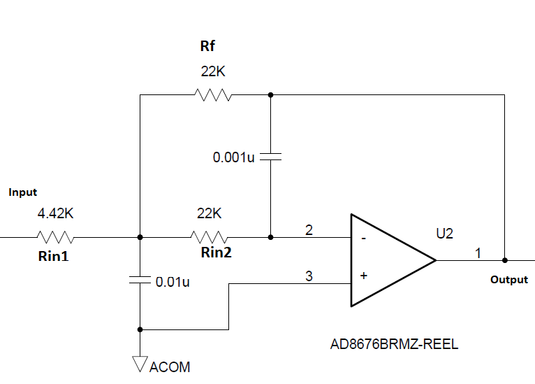
Op-Amp.png


If I could understand how does the 0.001uF and 0.01uF Capacitor is an advantage for this circuit it will be super.

thanks in advance.

Regards
 

Hi,

This is a filter, thus it has no "fixed" gain.
The gain depends on frequency.

For DC gain you may omit all capacitors. Remaining gain: A = -Rf / Rin1

Rin2:
* for DC there is no current through 0.001u
* there is about zero current into OPAMP_In-
Thus there is no current through Rin2.
--> no current flow, no voltage drop --> Rin2 may be ignored and treated as short circuit.

Klaus
 

    ash3

    Points: 2
    Helpful Answer Positive Rating
It's a second order MFB low-pass, 3 dB cut-off frequency about 1.3. kHz. Filter Q 0.45 lower than Bessel.
 

    ash3

    Points: 2
    Helpful Answer Positive Rating
1609252470216.png


A sim.

Regards, Dana.
 

    ash3

    Points: 2
    Helpful Answer Positive Rating
Hi KlausST, FvM & Dana,

Thanks for the respond, i appreciate it.
I have done some reading of MFB Low Pass Filters, and indeed it is a circuit used for ADC input application, as what i am using it for.
I can also perform simulation using this tool in this link

**broken link removed**

I am considering to open an option to use a different grade of op-amp for this circuit.
Currently im using B grade which have 60uV Offset voltage, while the recommendation is to use the A grade Op-amp that have a higher 100uV offset voltage.

1609729675303.png


Is there any way that we can quantify the impact of offset voltage to the performance of the MFB Low pass filter ?

Regards
Ashraff
 

Hi,

60uV offset is better than 100uV offset.
There is no impact on filter function.
Just the output_offset is expected to be (1 + 22k / 4.42k) × input_offset.

60uV input offset isn't that bad...but what are your requirements according offset voltage?

Klaus
 

    ash3

    Points: 2
    Helpful Answer Positive Rating
You have to be careful of offsets with gain blocks in front of ADC's. Depends on your requirements, there are low offset op amps. The more gain, the more any offset is amplified. There is even self zeroing op amps but they have some other entanglements as they periodically do self calibration that may not be totally transparent depending on application.
 

    ash3

    Points: 2
    Helpful Answer Positive Rating
Keep in mind Vos is not the only error you have to deal with.

One has to do an error budget end to end in the design if its a design seeking absolute
accuracy. PSRR, INL, DNL, Noise, T dependencies some of the gremlins you have to battle.

Regards, Dana.
 

    ash3

    Points: 2
    Helpful Answer Positive Rating
My ADC is a 24Bit ADC with 2.4V voltage reference.
ADC output.jpg


which means that the voltage change that will change the least significant bit [2.4V /((2^23) - 1) ]= 286nV.
However measuring the output of the ADC repeatedly with fixed voltage input before the MFB LPF, im getting ADC output range in the order of 2mV.
There could some other source of noise that i have not account for in this calculation.

regards
Ashraff
 

Hi,

Hopefully no breadboard test. Pleaee confirm. Show PCB layout.
What is this "fixed voltage input"? Where does it come from? What LPF?
What is the reference voltage source?
What gain and BW setup?
What sampling rate?

Noise:
Datasheet says 4uVpp at 150Hz BW, gain of 6, means more than 6 bits from the 24 bits are noise.

Klaus
 

Some useful ap notes on high precision, board layout. Attached.


Regards, Dana.
 

Attachments

  • AN280.pdf
    2.1 MB · Views: 153
  • AN57821_001-57821[1].pdf
    1.1 MB · Views: 256
  • sloa089.pdf
    171 KB · Views: 390

Status
Not open for further replies.

Part and Inventory Search

Welcome to EDABoard.com

Sponsor

Back
Top