Continue to Site

Welcome to EDAboard.com

Welcome to our site! EDAboard.com is an international Electronics Discussion Forum focused on EDA software, circuits, schematics, books, theory, papers, asic, pld, 8051, DSP, Network, RF, Analog Design, PCB, Service Manuals... and a whole lot more! To participate you need to register. Registration is free. Click here to register now.

[SOLVED] Effect of LC filter in simulation of BTL H-Bridge inverter?

Status
Not open for further replies.

Nurahmed

Junior Member level 1
Joined
May 27, 2019
Messages
19
Helped
1
Reputation
2
Reaction score
1
Trophy points
3
Location
Montreal, Canada
Activity points
172
Hi,
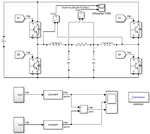
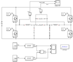
I am simulating this BTL configured H-Bridge inverter with BD modulation. When there is only a resistor load, the three-level PWM pattern is fine (VoutA-VoutB, resistor only). But after adding an LC filter, the PWM pattern is not correct (VoutA-VoutB, LC filter), the filtered sine wave is not correct too.

You can see the attached images for simulating schematics and waveforms. The LC filter value is calculated according to TI's filter design guide. I also tried setting initial conditions for L & C.

What could be the problem when adding the LC filter?
Thanks
FB_BD_resistor only.png
PWM_BD_resistor only.png
FB_BD_LC filter.png
PWM_BD_LC filter.png
 

Hi,

either your control schem or the dead time.

--> show all 4 gate drive signals in one screen.

Klaus
 

Hi,

either your control schem or the dead time.

--> show all 4 gate drive signals in one screen.

Klaus

Is it because of control scheme or the dead time? If it is, the pure resistive load PWM above would be wrong too, but that PWM is Ok. The control scheme is simple as compare reference sine signal with the triangle wave.
 

Hi,

Is it because of control scheme or the dead time?
We don´t know, that´s why I´m asking for show all drive signal. Now again.

If it is, the pure resistive load PWM above would be wrong too,
Wrong, because resistive load does not drive current/voltage but inductance do.

Klaus
 

Hi Klaus,

Here it is,

FB_BD_LC filter_Full.png
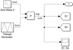
FB_BD_LC filter_S1_S4.png
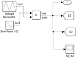
FB_BD_LC filter_S2_S3.png
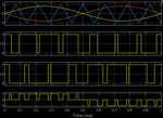
PWM.png

Two reference sine waves have 180 phase difference.
PWM principle.png
 

It's an unsuitable PWM pattern, driving only first and third output quadrant. To drive reactive loads with sine waveform, both half bridges must switch between high and low and never to off state.
 

It's an unsuitable PWM pattern, driving only first and third output quadrant. To drive reactive loads with sine waveform, both half bridges must switch between high and low and never to off state.

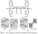
class d.png

This is one of the published paper, my pwm pattern is the same as BD modulation in the above figure.
 

Those capacitors to ground provide a direct path for damaging high current, if LC resonance was instigated by switching at certain frequencies.

---------------------------------------------

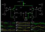
Here is my simulation of H-bridge applying SPWM to load via LC 2nd order filter. I believe it's the same as class D operation.

SPWM H-bri 4 mos 2 opamps 170VDC LC 2nd order load gets 120VAC sine.png

I put P-mos at the top so the biasing arrangement is easier. Furthermore I set bias voltage unrealistically high for mosfets.
 

Hi,

--> show all 4 gate drive signals in one screen.
Actually I can't find the requested screen.
Thus I can't verify the deadtime.

Generally S1 and S2 need to come from the same comparator with exact and low dead time.
(The same applies for S3 and S4)
I can't recognize this here.

Klaus
 
Those capacitors to ground provide a direct path for damaging high current, if LC resonance was instigated by switching at certain frequencies

In your simulation, aren't your comparators' input signs (left side & right side) are opposite to one another? i.e., if the left comparator non-inverting input is connected to the sine wave, then the right side connects to inverting input.

Is your modulation BD modulation? it looks AD modulation to me.

BTW, which tool do you use to simulate? the GUI looks very good :)

The screenshots are Falstad's animated simulator. Free to download and use at (your computer needs to have Java installed):

falstad.com/circuit

This is how the waveforms are produced by 2 op amps. Settings were edited so they produce only positive polarity. (However the inputs are exposed to negative polarity which is against guidelines in real life.) This is suitable to gate an H-bridge (receiving positive supply voltage).

SPWM produced by 2 opamps 2 sines 1 sawtooth.png

I believe it's BD modulation (per post #7 waveforms). The H-bridge duplicates the action of a buck converter in one direction during one half of the cycle (through Q1 Q4, post #8).
Then it reverses current flow and becomes similar to a buck converter in the opposite direction (through Q2 Q3) during the other half of the cycle.
 
This is one of the published paper, my pwm pattern is the same as BD modulation in the above figure.
It's not the same PWM scheme. It's using the same kind of signal generation, but is driving the switches differently.

S2 e.g. should to be driven with inverted S1 signal. A small dead time has to be applied to S1 and S2, can be generated by delaying the rising edges.

The criterion is to get full VoutA and VoutB swing independent of the output current polarity. S1 and S2 must be operated in push-pull manner to achieve this.
 
It's not the same PWM scheme. It's using the same kind of signal generation, but is driving the switches differently.

Thanks a lot. I've made a mistake with the driving scheme. Now I got the correct results.

S1.png

S3.png

FB.png

PWM_waveform.png
 
  • Like
Reactions: FvM

    FvM

    Points: 2
    Helpful Answer Positive Rating
Status
Not open for further replies.

Similar threads

Part and Inventory Search

Welcome to EDABoard.com

Sponsor

Back
Top