Continue to Site

Welcome to EDAboard.com

Welcome to our site! EDAboard.com is an international Electronics Discussion Forum focused on EDA software, circuits, schematics, books, theory, papers, asic, pld, 8051, DSP, Network, RF, Analog Design, PCB, Service Manuals... and a whole lot more! To participate you need to register. Registration is free. Click here to register now.

Synchronous Buck Converter FET selection

Status
Not open for further replies.
Unless you have a 200MHz scope and high quality scope probes - you may not see the true rise and fall times - have you calibrated your probes? - via the 5V square wave on the scope

Fet temp rise is very heatsink dependent - and air flow dependent - 60-65 C on the fets is usually regarded as a good result at full power ...

- - - Updated - - -

else - that is the best the chip can do -
 

Same remark as Easy Peasy, 60 - 65°C is not bad at all, it's a great improvement since your first post. I still recommend you to calculate the theorical power dissipation in your MOSFETs, and then compare the result with the temperature you are measuring.

The evaluation board for this IC (DC674B) is a 4 layer PCB with 2Oz external and 1Oz internal, what stackup do you use for your PCB?

There is no thermal via under your MOSFET dissipation pads, you could add it in the next version (if there is another plane under that can conduct the heat).
 

EP,
That is a good point. I just checked the 5V sq wave at the same horizontal resolution and I get 400ns+ fall times so I am probably reaching the limitations of this scope.

I guess it would be helpful to have an eval board to compare waveforms to.

I was able to talk to an applications engineer at Linear (Analog) and they did not see anything obvious wrong with my layout or FET selection.
The Eval board has an SO-8 optional FET footprint over the top of the SuperSOT-6 footprint. I assume this is for increasing the power output capability of the board.
DC674B-4.jpg

I was hoping to find out what specific FET the footprint was added for (normally it would be shown as an optional part in the schematic) but they did not have one specifically called out.
Analog suggested STS6P3LL6, which is very similar to the P-FET that lipitimisieu mentioned.


My concern with 60C temperatures is that this is on the bench with ambient around 25C in open air. This board will be enclosed (with fans) and operating in ambients up to 35C.
I guess like you said, I will need to focus on heat dissipation rather than efficiency now.

My board stackup is only 2 layer. Prototypes are 1oz but production will be plated up to 2oz. The thermal vias surrounding the FET pads transfer heat to the bottom layer of the PCB which also gets around 55-60C so there should be enough thermal vias.
The bottom of the PCB will be mounted to a plastic (G10) panel with only about 3mm spacing so I need to focus on heat dissipation on the top side to prevent excess buildup underneath.

The copper pour shared by the drains of both FETs is about 0.66 sq-in top and bottom. Now that I say that, the Rth-ja given is for 1 sq-in and I'm sharing this thermal pad with two FETs so I probably need more like 2 sq-in of 2oz copper to get the rated Rth-ja of the FETs.

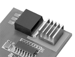
I'm finding products available for surface mount heatsinks rather than case mount heatsinks like this:
bild1.gif

Because of the poor thermal connection to the plastic case of the FET, would this style be better at dissipating heat?

Thanks


I can add large heatsinks to the top of the FETs but it may not help if
 

There are linear.com sync buck drivers which have bootstrap drive for a top side nfet, and these I think are better.
You always need a series gate resistor , as EasyPeasy said, even if you end up zer0-ohming it…..also to reduce problem of esd damage to fets, your better with a 10k gate-source resistor too.
You should be able to do this and get pretty cool running fets , so you are right to be concerned….as EasyPeasy also said, you also need parallel schottky in parallel with your low side fet……….then what you can do, to investigate if shoot through is prevalent………you can remove the low side series gate resistor……put a zero ohms from gate to source to keep the low side fet off…then just run it through the schottky, which will give far less shoot-through…and you can see how that heats.
Also, did you manage to properly solder the heat pad of the fets to the footprint?
Linear.com have loads of sync buck drivers with fully working ltspice models, so it’s a shame you don’t use one of those……..i am just wondering if your top side fet drive is too weak…..as the vgs didn’t look too snappy….of course, as you know, a too quick vds rise and fall time can sometimes cause noise….and one of the uses of the series gate resistor is to dampen the switching so as to reduce this noise.
What about buying one of these so you can see the heat of the fet…..HT-04 thermal cam by HTI
https://uk.banggood.com/HT-04-220x1...MI-pWc34e04wIVxrTtCh0mIgHxEAYYASABEgL1vvD_BwE

Resolution not great but good enough.

- - - Updated - - -

Also, what is the model no of your scope to check the bandwidth, and also check the scope probes make and model.

- - - Updated - - -

Also, regarding your smt heatsink of #23 above, i bet that would be better if it was thermal glued to the plastic case of the dpak.........the way the pic shows, the heat has to get along the thin film of pcb copper to even get to that heatsink....better on the plastic case......especially some fets where the plastic case is thin and you can get the heat out better......there used to be smt fets with metal tops so you could heatsink to them...but theyre all but gone now.

- - - Updated - - -

But yes your switching period is some 2.25us, so you want a fast switching vds so your not consuming too much of the sw period in I/V overlap.
 
There are linear.com sync buck drivers which have bootstrap drive for a top side nfet, and these I think are better.
You always need a series gate resistor , as EasyPeasy said, even if you end up zer0-ohming it…..also to reduce problem of esd damage to fets, your better with a 10k gate-source resistor too.
You should be able to do this and get pretty cool running fets , so you are right to be concerned….as EasyPeasy also said, you also need parallel schottky in parallel with your low side fet……….then what you can do, to investigate if shoot through is prevalent………you can remove the low side series gate resistor……put a zero ohms from gate to source to keep the low side fet off…then just run it through the schottky, which will give far less shoot-through…and you can see how that heats.
Also, did you manage to properly solder the heat pad of the fets to the footprint?
Linear.com have loads of sync buck drivers with fully working ltspice models, so it’s a shame you don’t use one of those……..i am just wondering if your top side fet drive is too weak…..as the vgs didn’t look too snappy….of course, as you know, a too quick vds rise and fall time can sometimes cause noise….and one of the uses of the series gate resistor is to dampen the switching so as to reduce this noise.
What about buying one of these so you can see the heat of the fet…..HT-04 thermal cam by HTI
https://uk.banggood.com/HT-04-220x1...MI-pWc34e04wIVxrTtCh0mIgHxEAYYASABEgL1vvD_BwE

Resolution not great but good enough.

Thanks treez, I wanted to keep the gate traces as short and away from other components as possible so adding 0-ohm resistors and pulldowns/pullups makes layout harder. I really like the idea of adding a parallel diode and removing the gate resistor to check for shoot-through. I will do that on all designs going forward to make the testing phase easier.
On most Linear converter evaluation boards, they have 0ohm gate resistors like you say, but this evaluation board does not have them so I decided to also leave them out.

Thermal camera is high on my list of things to get. All I have right now is a IR thermometer so I can take average surface temperature but not pinpoint. Have you used the HT-04 camera before? Is it reasonably useful or junk? Thanks

The reason I selected LTC4011 is that it is meant for NiMH fast charging and can accept higher than 24V input (my power supply is 24V nominal). Between Linear and Texas Instruments, I couldn't find any other NiMH buck charge controller that has programmable voltage up to 10S (~12-15V) battery and >24V input. All other charge controllers I found are 1-4 cell output.

Also, what is the model no of your scope to check the bandwidth, and also check the scope probes make and model.
Scope is Siglent SDS 1102CML 100Mhz 1GSa/s
Probe is TP6100 100Mhz probe
I also have PP510 100Mhz probes to use if they are better but they feel cheaper.

Also, regarding your smt heatsink of #23 above, i bet that would be better if it was thermal glued to the plastic case of the dpak.........the way the pic shows, the heat has to get along the thin film of pcb copper to even get to that heatsink....better on the plastic case......especially some fets where the plastic case is thin and you can get the heat out better......there used to be smt fets with metal tops so you could heatsink to them...but theyre all but gone now.

But yes your switching period is some 2.25us, so you want a fast switching vds so your not consuming too much of the sw period in I/V overlap.

Thanks! I am making my PCB larger and it will be 2oz instead of 1oz copper and also adding a small cooling fan. I really do not want to add a cooling fan but I can always remove it if it's unnecessary. When I tested the board inside an enclosure, the board surface reached 70C+ but when a small fan was running, temp decreased to 38-39C (board temp, not FET temp).

I have no problem using through-hole FETs with larger heatsinks but I could not find any FETs that seemed comparable. Gate charges were all very high.

- - - Updated - - -

I know of these FETs with metal top surface but they all have gate charges way too high for this chip
https://www.onsemi.com/pub/Collateral/FDMT80060DC-D.pdf

Also infineon makes a lot of metal cased MOSFETs but I did not look into those at all
 

Update - I've gone back to my previous board design with D-PAK (TO-252) FETs and have installed STD52P3LLH6 and STD65N3LLH5

P-FET:
Qg= 33nC @ 4.5V
Rds-on = 17mR max

N-FET:
Qg = 3.6nC @ 4.5V
Rds-on = 9.3mR max

With a small adhesive heatsink and cooling fan running directly over it, they stay very cool now.

I've been able to increase my charging current up to ~5A (4.87 measured) and I'm getting a measured efficiency of 87.0% (should be better?)
The LTC4011 graph shows efficiencies up around 90-95% when Vin = 20V and Iout = 2A

So I'm wasting/dissipating around 9.9W of heat and the bottom surface of the PCB is maintaining about 30C at 22C ambient (with no thermal vias on this version).
Maximum power dissipation rating of the P-FET and N-FET are 70W and 50W respectively so I should be well within operating limits.

I now need to add a fan control switch to the PCB and an overtemperature power cutoff switch (in the case the fan fails).
What's the most cost effective way to create overtemp cutoff?
(Edit - with only a 24V rail)
 
Last edited:

measuring efficiencies is very problematic, you need better than 0.5% instruments to get near a 1% error, even so it is likely your eff is a little higher than you think - pretty good for a first off effort...

- - - Updated - - -

what parts did LTC use in their version ..?
 

LTC's DC674B Eval Board uses PFET FDC658AP and NFET Si3434DV and has max output of 2A and 10-cell battery.

My goal was 5A charging so I can achieve that now, but only with active cooling. I still think this should be possible to do without active cooling and below 60C but I would probably need a bootstrap n-fet driver.

Once I get more functioning boards built, I will test what happens when active cooling is removed (in case of fan failure). The FETs are technically rated operational up to 175C (Tj) but I'm guessing they will fail much faster.
 
  • Like
Reactions: treez

    T

    Points: 2
    Helpful Answer Positive Rating
Surprisingly the fets will work up to 125 degC without issue - but the accompanying rise in Rds-ON, with contant current operation will likely cause thermal runaway.

Please note that the watt rating of fets is given for the tab being held at 25 degC, linearly reducing to zero watts at max junction temp on the tab - it pays to read the data sheets carefully ...
 
  • Like
Reactions: treez

    T

    Points: 2
    Helpful Answer Positive Rating
Status
Not open for further replies.

Similar threads

Part and Inventory Search

Welcome to EDABoard.com

Sponsor

Back
Top