Continue to Site

Welcome to EDAboard.com

Welcome to our site! EDAboard.com is an international Electronics Discussion Forum focused on EDA software, circuits, schematics, books, theory, papers, asic, pld, 8051, DSP, Network, RF, Analog Design, PCB, Service Manuals... and a whole lot more! To participate you need to register. Registration is free. Click here to register now.

current mirror matching issue

Status
Not open for further replies.

Junus2012

Advanced Member level 5
Joined
Jan 9, 2012
Messages
1,552
Helped
47
Reputation
98
Reaction score
53
Trophy points
1,328
Location
Italy
Activity points
15,235
Dear friends,

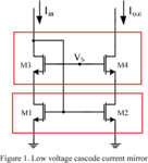
Attached is an image of the simple wide swing current,

in layout I am matching M1 with M2 in one group, then I match the M3 and M4 separately in other group, then I put M3-M4 above the M1-M2

My question is, can I put the matched transistors M3-M4 beside the matched transistors M1-M2 ?

Thank you very much
mirror.png
 

That should be fine but you’ll want to keep them close together. The important part is that M1 matches well to M2 and that M3 matches well to M4 and MB. You won’t really be able to place them in the same well if your cascode devices are source body tied anyways. Depending on how precise your matching needs to be, you can either just place them next to each other, or create 2 groupings of the top devices and 2 groupings of the bottom devices (devices+wells/guard rings) and common centroid that. Be sure to use dummy devices as well.

Edit:

Not sure what your application is, but if you’re going to be running several mA through the current mirror, I find it’s a lot easier to meet electromigration if you stack them vertically. Create a lot of parallel traces on the lower level metals and cross hatch up to a bigger metal higher in the stack. That helps distribute current evenly and reduce overall stripe current density in the current mirror. At high currents it’s pretty important to make sure that the traces are well matched in the sources of the lower devices.
 
Last edited:
Is the reason you want to keep them side by side rather than above-below, because the area you have longer horizontally than vertically?
 
Thank you friends for your reply

I am using it for small currnt of 50 uA

The reason is just to fit the space in my layout, otherwise I usually follow the vertical connection
 

The best option is to keep transistors in stack abutted. It makes layout the most compact in this case.
 
You can abut them but this comes with some limitations. The width of the cascode devices should be the same as the width of M1/2 in order for this arrangement to work. Also, if you have multiple fingers per device it becomes more inconvenient to abut them. So, not unusual to see people organize M1/2 and M3/4 in different groups and just connect them in metal.
 
Actually there is a simple solution for this.

Assume Mbias W/L = 3/5 (Long Length for matching)
Assume Mcascode W/L = 1/1 (Some Min Length)

Use the unit W = 1

And place the devices in one diffusion of width = 1, Sb-----Db Db-----Sb Sb-----Db Sc-Dc (Each - reperesents 1u Lengh)
Sb = Mbias Source, Db = Mbias Drain
Sc = Mcascode Source, Dc = Mcascode Drain.

To do this you need Odd number of fingers in Mbias and same widths for Bias and Cascode (As long as some sub units have the same widths, that is also good enough).

With this as a unit, you can do the rest of the matching pattern and not worry about routing between the Bias and Cascode groups.
 
You can abut them but this comes with some limitations. The width of the cascode devices should be the same as the width of M1/2 in order for this arrangement to work. Also, if you have multiple fingers per device it becomes more inconvenient to abut them. So, not unusual to see people organize M1/2 and M3/4 in different groups and just connect them in metal.

indeed most of the people are matching them in different groups, you can see the design problem 12.15 in the book of "The art of analog layout". Also in one of your suggestion in other post you have kindly stated that the design constrains for the top transistors are less compared to the real mirror transistors
 

Status
Not open for further replies.

Part and Inventory Search

Welcome to EDABoard.com

Sponsor

Back
Top