Continue to Site

Welcome to EDAboard.com

Welcome to our site! EDAboard.com is an international Electronics Discussion Forum focused on EDA software, circuits, schematics, books, theory, papers, asic, pld, 8051, DSP, Network, RF, Analog Design, PCB, Service Manuals... and a whole lot more! To participate you need to register. Registration is free. Click here to register now.

Input offset voltage simulation for the fully differential operational amplifier

Status
Not open for further replies.

Junus2012

Advanced Member level 5
Joined
Jan 9, 2012
Messages
1,552
Helped
47
Reputation
98
Reaction score
53
Trophy points
1,328
Location
Italy
Visit site
Activity points
15,235
Dear friends,

could you please tell me how to simulate the input offset voltage of the fully differential amplifier,

the second question is how we can compensate for the offset voltage by while we have common mode feedback loop which always control the currents.

Thank you very much
 
First set up a test bench where your two inputs are offset by a certain parameter (lets say voffset). Run a dc-sweep simulation where you sweep the voffset from a sufficiently low enough negative value to a large enough positive value. Write expression to find out at what value of 'voffset' your two outputs (positive and negative) become equal. Now run a Monte carlo simulation to see the distribution of our input referred offset.
 
Thank you vivo, this method is looks like the simulation setup for the single ended opamp,

but i didnt understand the part why you want to run the monticarlo analyses now? what you mean to say by seeing the distribution of the referred offset

thank you once again
 

The input referred offset always has two components -- systematic and random. For the random, you need to do MC analysis.
But it is of a fully differential op-amp... Only a fully differential op-amp has two outputs -- positive and negative,,
 

one more question please,

how we have offset voltage when we have a common mode voltage circuit, the CMFB should compensate the offset voltage to zero
 

Dear FvM,
I understand by the error in the differential voltage signals when they both not intersecting at at the desired value of VCM.
now if the outputs are not intersecting at VCM, will you say it is because the offset voltage error or because the CMFB loop need more accuracy.

if the reason will be related to the CMFB loop then one can increase the common mode feedback amplifier gain,
if the reason is related to the offset voltage then one at least have to apply compensated input voltage

that is what I am thinking and looking forward to your reply
 

If (Vout,p + Vout,n)/2 != Vcm_out,desired ==> you have a common mode feedback problem
If Vout,p!=Vout,n when Vinp,p == Vinp,n ==> you have offset. This offset has nothing to do with common mode feedback. Your common mode feedback circuit can only change the value of {(Vout,p + Vout,n)/2}

P.S. Its not trivial to go for a very high gain of your common mode feedback amplifier as you will run into stability issues for sure (poles in your main amplifier + poles due to CMFB amplifier).
 
  • Like
Reactions: Junus2012

    Junus2012

    Points: 2
    Helpful Answer Positive Rating

    KEY98

    Points: 2
    Helpful Answer Positive Rating
Thank you guys for your help,
for unknown reason i am not able to vote for help at your replies,

I attached you my result of simulation,

As you can see that my two output signals are exactly intersecting when vin+ = vin- (in the graph at X=0 which means (Vin+)-(vin-) =0. According to what I understand from you it means I have zero offset voltage,

now the value of the output voltage (Vo+, Vo-) is equal 1.6428 V , instead of 1.65 V of the desired VCM,

now the problem is CMFB ???

off.png

thank you gain
 

If I remember well, your CMFB input is a "gm over gm" stage, a diode loaded diff.amp. This has got low gain, which can result in higher CMFB gain error. CMFB loop gain has to be checked as the main amplifier too in AC or stability analysis. Not always good that the CMFB amlifier has got low error from the expected common mode voltage, in your case it is n*10mV which you lost from output headroom. You can deal with that if the stability is just good enough.

P.S.: cadence schematic + testbench + annotated parameters, operating point. Make your life easier, and share these.
 

I am sorry again for not able voting for help i dont know why ,

Dear frank, the error of the output VCM is 1.65-1.6428 = 8 mV which is very accepted for my case, yes you are right if would increase the gain of ther CMFB i will get better VCM but i might scarify the stability.

you mentioned one important point that I must simulate the common loop feedback stability, indeed i posted this issue in other post but i didnt get a reply,

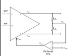
if you refer to the following circuit diagram of the op-amp can you please tell me how to simulate the CMFB closed loop parameters (PM, GBW).

I can tell you that I measured the CMFB closed loop gain from DC analyses by sweeping the VCM and recording the Vo+ and Vo-, by taking the derivative of the output is giving me a gain equal to 0.999 which almost perfect. under this simulation both of the input voltages where kept at 1.65 V and the amplifier is in open loop condition.

Thank you once again
I am looking forward to your reply

kkk.png
 

Status
Not open for further replies.

Part and Inventory Search

Welcome to EDABoard.com

Sponsor

Back
Top