Continue to Site

Welcome to EDAboard.com

Welcome to our site! EDAboard.com is an international Electronics Discussion Forum focused on EDA software, circuits, schematics, books, theory, papers, asic, pld, 8051, DSP, Network, RF, Analog Design, PCB, Service Manuals... and a whole lot more! To participate you need to register. Registration is free. Click here to register now.

fully differential amplifier based on folded cascode topology with class AB buffer

Status
Not open for further replies.

Junus2012

Advanced Member level 5
Joined
Jan 9, 2012
Messages
1,552
Helped
47
Reputation
98
Reaction score
53
Trophy points
1,328
Location
Italy
Activity points
15,235
Dear Friends,

I finished with the design of the folded cascode amplifier with resistive load push pull driver, the circuit I used is given by Jakob book and I attached you here,,
Now I need to convert it to fully differential amplifier based on the same topology,

I have searched but didnt find a resource describing how to make this circuit fully differential

I would appreciate very much your help and thank you in advance

best regards folded buffer.png
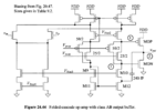
 

Your power supply appears to be single-ended positive polarity.
You input section (at left) appears to be a differential amplifier (I think).
I suppose you ought to clarify:

* Do you want a second output stage which voltage rises or falls in the opposite direction from the first output?

* Or do you want a second output stage which is negative polarity when the first output is positive (and vice-versa)?
 

Meaning of fully differential is obvious I think, differential input and output.
For this in the 1st stage you have to disconnect diode-connections = disconnect M11 gate from M9 drain, and do the same for the PMOS transistors above.
You have to choose, create a common-mode feedback (CMFB) topology/circuit, which can control the gate of M11 for example, and connect the floating PMOS gates to a bias, reference voltage.
What is missing that you have to add the replica of the output stage of above figure to the other side, compared to where they connected currently.
For CMFB and FD OPAmps I recommend "Analysis and Design of Analog Integrated Circuits" from Gray/Hurst/Lewis/Meyer.
 

Dear Bradthred, dear frank

Thank you for your help,

I have found this modification attached the image if it here,

it exactly do what you told frank and this is the circuit I want guys,, the only thing confusing me is that he is using complicated CMFB,
you suggested me to read the book of Gray Meyer and indeed this book use very clear to understand CMFB,

So can I use the CMFB from gray in this circuit ?

fully differential.png

CMFB.png

Thank you again
 

Probably you could, but figure reveals the main issue of the Johan Huijising book. He sometimes uses dots at crossing wires, sometimes not on the same figure... annoying, I am not sure this is from Gray's book.
 

it is confusing me as well, specially i am using pmos and nmos input stage
 

I think the amplifier in Huijising book (the fully differential one) i s missing a connection of the drain of M32 to the source of M46 - the same way it is done for M31 and M45.
 

The CMFB works this way. Rcm1's sense output common-mode voltage which it is attached to the source of M51 and M52. The gates of M51 and M52 are at the same and constant voltage, generated by the diode-connected transistor M53. If the CM output voltage goes up, then VSG51,52 goes up, and transistors M51 and M52 inject more common-mode current at the folding node (sources of M45 and M46), which decreases the CM output voltage. That's the way that the CM negative feedback works.

Regarding your last question, yes! you can use whatever CMFB topology you want, as long if it is able to meet the require specs of your design. When doing CMFB designing, your principal concerns are: 1) CMFB input range which limits the output swing of the amplifier and 2) stability of the CMFB.
 
Thank you dears,
The circuit with CMFB secondly presented by Huij is different from the first one by Jakob,,,
I am working with the circuit from Jakob which has NMOS and PMos differential input stage and hence have two mirrors as the output, this is the point why I am confused in my design,
 

    ARAMIC

    Points: 2
    Helpful Answer Positive Rating
Status
Not open for further replies.

Part and Inventory Search

Welcome to EDABoard.com

Sponsor

Back
Top