Continue to Site

Welcome to EDAboard.com

Welcome to our site! EDAboard.com is an international Electronics Discussion Forum focused on EDA software, circuits, schematics, books, theory, papers, asic, pld, 8051, DSP, Network, RF, Analog Design, PCB, Service Manuals... and a whole lot more! To participate you need to register. Registration is free. Click here to register now.

Rail to rail input-output fully differential Op-Amp with class AB buffer driver

Status
Not open for further replies.

Junus2012

Advanced Member level 5
Joined
Jan 9, 2012
Messages
1,552
Helped
47
Reputation
98
Reaction score
53
Trophy points
1,328
Location
Italy
Activity points
15,235
Dear Friends,

I am converting the attached circuit to fully differential version of it, but it is not working with me, may be the circuit have two mirrors at the output, i am simply converting the up and down mirrors to current source and connecting CMFB to the down one, but the circuit is not functioning,

I would appreciate your help if you could suggest me the procedure for modifying the circuit to fully differential output

Attached you find please the circuit of the single ended output so you can refer to it in your explanation
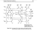
Fully differential amplifier.jpg

Thank you very much in advance
Best Regards
 

Don't you want to show your drawn circuit rather with the CMFB? With DC annotations of node voltages and operating points, to see why not working. Maybe it would be easier to repair it.
 

Don't you want to show your drawn circuit rather with the CMFB? With DC annotations of node voltages and operating points, to see why not working. Maybe it would be easier to repair it.


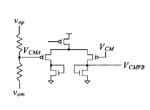
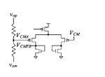
here the circuits for both the differential and the CMFB

fuuly2.jpg

CMFB.jpg
 

Hi Junus,

can you show simulations of what isn't working? As frankrose said above, it would be useful to give DC annotations, in order to check whether the transistors are operating in the active region. Here some notes:

1) Since you are designing a fully differential architecture, no single-ended conversion is made at the current mirrors. Transistors sizes and biasing provided by Baker are for the single-ended version, so I suggest you to revisit and check those design choices, properly for a fully differential architecture. Maybe you are not properly biasing the top and bottom current sources and they are working in the triode region.
2) what kind of simulation are you doing? If you are testing your circuit with large signals, you are missing an auxiliary circuit at the input (according to the schematic you provided), which maintains the input transconductance constant over the input range, since you are using a complementary input stage.
3) I recommend you to deal with CMFB later, when differential mode is correctly designed. So you can test your circuit using an ideal CMFB.

Wish you the best with your design!!
 
Thank you matias for your reply

actually now I am simulating without a CMFB circuit, what I have done is I broke the diode connected in the mirror and connected them as a current source transistors biased by a biasing voltage,

this biasing voltage i took it from the simulation of the single ended version of the circuit, I checked the currents for the fully differential version and it is comparable to the single ended one. I am getting two ideal complementary outputs but they are not intersecting to each other. Ideally they must intersect at VCM = VDD/2, however since I didnt connect the CMFB they are will not be perfect but for me they are not intersecting at all.

When I will go to the lab i will provide you with the simulated outputs to make it more cleare

Thank you again
 

Hi Junus,

it seems that the problem is related to the CM output voltage which is not well defined. Since the output of the first stage is very high impedance, little changes in the current would change the CM output voltage considerably. Also, in the single-ended version, the current is defined by a floating current source which is mirrored at the top and bottom of current mirrors. In the fully differential circuit, these two middle transistors work as a class AB bias generator for the other half side of the circuit (and they are no longer a floating current source), and the current is defined by the top and bottom active loads, so they need to be properly biased. Maybe the difference between the top and bottom active load currents is significant moving the CM output voltage upwards of downwards.

1) Run a .DC sweep to find the proper bias voltage of those transistor so the top and bottom currents are matched.
2) Add an ideal CMFB feedback loop (calculate the CM output voltage using ideal Voltage dependent voltage sources and amplify the error using an ideal VCVS too and feedback these signal to the bottom or top active load. Remember that this signal must have the DC bias component in order to properly bias the active load at the designed operation point). From the figures you provided, lets call the bottom active load transistors M6 (which are controlled by the feedback signal Vcmfb as shown in the schematic you provided above). So Vcmfb = VGS6_DC + Acmfb*Vocm, where VGS6_DC is the bias voltage of M6 which gives you the desired CM output voltage for zero input, Acmfb is the gain of the CMFB loop and Vocm is the measured CM output voltage. If you already defined VGS5_DC for the top active load transistors M5, then you can find VGS6_DC running a .DC sweep as I told you before in order to obtain the desired CM output voltage (assuming that transistors sizes are already given).
 
Dear Matias,

I highly appreciate your nice way of explanation things, very useful information.

As I promised , I will support my problem with the DC simulation (which you also suggested ) so we could find if there is other problem

Thank you a lot.

- - - Updated - - -

Dear Matias, Dear all friends,

I just came to the lab to show you the DC open loop simulation,

in the first pictures it shows how correctly the circuit is giving me perfect complementary differential output by applying differential input signals,

in the next picture I zoomed the first graph to show how they are not intersecting at all,

Note: I run this simulation without a CMFB circuit

DC1.png

DC2.png
 

Hi Junus,

it seems that you have a problem with the Class AB bias generator. If you plot Vod vs Vid, there is little range for Vid (centered at 0) where Vod = 0, generating crossover distortion. Maybe you are not properly biasing your output transistors, so there is a little range where neither side is conducting.
 

Without CMFB fully differential OPAmp cannot work, the point of CMFB to set normal active region for amplifier and current source devices. Not a surprise it cannot operate as an OPAmp. At zero differential input the outputs are 0V, some of your devices are in triode region proably. Connect CMFB and show DC annotation of operating points and node voltages. Ideal or non-ideal, just connect it please.
 

Dear friends,

I will connect the CMFB then I will show you the result,

Thank you for the suggestions, I appreciate your help so much
 

Dear friends,

I designed the CMFB amplifier based on the circuit I posted before. I chose the value of the resistors of the CMFB as large in order to avoid any trouble.

After running steady state DC operating point simulation, I checked that every transistor is working in the saturation region, currents are perfectly balanced in every branch, every value is fully comparable to the single ended version of the same circuit.

However, when I run the open loop DC transfer simulation the output is stuck on zero and not giving any change with sweeping the input voltage. I couldn't find an explanation or reason for this case, therefore I would like to ask for your kind help if you can suggest me some solutions or advice.
 

Could you show your testbench? How does this DC open-loop simulation looks like exactly? This information you shared simply not enough.
 

    V

    Points: 2
    Helpful Answer Positive Rating
Dear frankrose,
Dear all

I have fixed the issue, the circuit is working now perfectly with the DC sweep as you can see by the attached graph,

I fixed the problem accidentally by moving the control signal of the CMFB from right to lift as shown below in the circuit

Now I only need to know an explanation for it how this CMFB is regulating the output please

thank you very much

CMFB.jpg

OTC.jpg
 

How the CMFB operates you should know before design, don't you think? There are lot of explanations in the literature, we cannot provide you better explaination than those. We can just help you to answer specific questions about the details, or give advices to solve issues, practical recommendations and so on. I have already suggested to you I think the Gray/Meyer Integrated circuit design book, that is very good explaination.
 
Yes Frank I read that book and those literature you suggested, but they connect the CMFB to the right which was not working with me,,, now when I changed it it is working...

May be in these books they dont have the floating transistor for the push pull driver, and now when I have it in my design I should reverse the operation of the CNFB control,

so when the output common mode voltage is increasing my CMFB amplifier decreasing the down current and so the current through the class AB floating transistors which is leading to decrease the output common mode voltage to the level of VCM
 

Dear friends,

The last simulation i showed to you was when the closed loop gain is equal to three... circuit working perfectly.

But when I am connecting it in unity gain configuration and sweeping the differential input I am getting the output shown below.

in the graph the x axis represent the differential input voltage (vin1-Vin2).

You can see from graph that the output is not linear for the all input range (it start to bend about +- 580 mV) which I dont understand because i am using rail to rail input stage

Thank you in advance

VTC_InAmp.jpg
 

Hello frank,

I am using this setup,

Actually I have connected additional differential pairs to make use of what so called differential differential amplifier, it is basically is as same as fully differential amp but provide non inverting output

fully diff.jpg
 

First, this setup is a figure from the Gray,Meyer book, not your testbench. I understand if you don't want to share a print-screen, but it will limit the efficiency of solving.
Second, I don't see how you added the additional diff.pairs, this is not a simple unimportant detail I think, now you are talking about an other circuit basically.

Show more information about your circuit, how you connect the additional transistors, maybe you missed a connection somewhere, or how you modified the common-mode feedback (I've just assumed you had to). Or if you don't want to share more, I recommend you to check which transistor is not in saturation when your phenomenon occurs. Non-linearity of OPAmps is strongly connected with decreased open-loop gain, which is connected with devices which entered into triode region. You can set a DC input value and save operating points at that, annotate the regions to the schematic.
 
Dear Frank

i didnt share the circuit not because i dont want to share it, but because i am not in the city of my university, however the setup from the gray is exactly the same setup i am performing, i am applying differential input voltage and sweeping it and getting the output.

i already checked the transistors for the operating point and all working in sat, for sure at the non linear part of my graph some of them will be triode.

the non linearity you mentioned about with decreasing the loop gain is not the case of my situation since I am running dc simulation where the gain is highest, that what you talk about is when applying an ac signal with high frequency.

for the circuit when i comeback to my city i will print it from my computer .

but sine you you know the idea is from gray i can tell you that i did exactly as same he did in this picture but for my folded amp

gray.jpg
 

Status
Not open for further replies.

Part and Inventory Search

Welcome to EDABoard.com

Sponsor

Back
Top