Continue to Site

Welcome to EDAboard.com

Welcome to our site! EDAboard.com is an international Electronics Discussion Forum focused on EDA software, circuits, schematics, books, theory, papers, asic, pld, 8051, DSP, Network, RF, Analog Design, PCB, Service Manuals... and a whole lot more! To participate you need to register. Registration is free. Click here to register now.

S11 is larger than 0dB

Status
Not open for further replies.

shanmei

Advanced Member level 1
Joined
Jul 26, 2006
Messages
430
Helped
8
Reputation
16
Reaction score
8
Trophy points
1,298
Location
USA
Activity points
4,496
If an antenna is terminated at 50 ohms, then the S11 is less than 0DB.


If an antenna is terminated at a complex impedeance (50-500*i) ohm and the termination is passive as well , is it possible that the S11 is greater than 0dB for certain frequency range? Thanks.
 
Last edited:

No. Negative s11 dB number (|s11| > 1) corresponds to negative resistance, not possible for passive circuits.
 
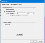
I think I have not renormalized the impedance.

Usually, the port impedance is 50 ohms, so we do not have to choose the renormalize option.

If the port impedance is not 50 ohms, then we should choose the normalize option otherwise the complex port might have positive S11.

I really appreciate your rely.

Capture.PNG
 

No. S11 of passive circuits always stays inside the unit circle (|S11| <= 1, S11db <= 0), for any real reference impedance Z0.
 
For real reference impedance port , for example Z0=50 ohm, S11dB <0.

For complex impedeance port, for example, Z0=50+500j ohms, S11dB migth > 0 . right?

The complex impedance should not be normalized toi 50 ohm.
 

For real reference impedance port , for example Z0=50 ohm, S11dB <0.

For complex impedeance port, for example, Z0=50+500j ohms, S11dB migth > 0 . right?

The complex impedance should not be normalized toi 50 ohm.

We discussed this phenomena in this forum few times.
Your fault is to fix the Characteristic Impedance being as 50 Ohm.Essentially your Characteristic Impedance is not 50 anymore and S11 cannot be calculated as usual.
Instead it should be calculated as

S11=(ZL-Conj(ZS))/(ZL+ZS)
 
For complex impedeance port, for example, Z0=50+500j ohms, S11dB migth > 0 . right?
I didn't calculate, I guess yes. But I don't a see reasonable physical meaning of complex reference impedance. Please enlighten me if you can.
 
But I don't a see reasonable physical meaning of complex reference impedance. Please enlighten me if you can.

Let me answer you..
In fact there is no complex Characteristic Impedance in real world except some very lossy mediums ( what Textbook says..)
In additional to, some few textbooks cover this phenomena and it's not very detailed explained and been passed as is..
 
For example, the matching between the RFID chip and the RFID antenna.

The output impedance of the RFID chip is 50-500j, then the antenna input impedance should be 50+500j for conjugated matching.

Now I am designing the antenna with the port impedance set to 50+500j in HFSS.

The RFID chip always has an imaginary impedance part.
 

Reflection always comes together with characteristic impedance of a transmission line. In your case, the load impedance is 50+j500, source impedance is 50-j500. While they are connected together without any delay. In this situation, reflection doesn't make any mean anymore. Reflected signal must travel in the opposite transmission direction of the signal, you have no way to distinguish the direction of signal since the delay is zero.

While if you put a transmission line between the source and load, there exists delay and it makes the reflection meaningful.
 
The output impedance of the RFID chip is 50-500j, then the antenna input impedance should be 50+500j for conjugated matching.
Now I am designing the antenna with the port impedance set to 50+500j in HFSS.


In your design, include the feed of antenna; and the cable in between as well. It's never a perfect match between chip and antenna; you need to add delay components and lossy parts to make matching work. As others have stated before, reflection makes sense when there are space to reflect.

You can check the concept of using lossy cables(or tapered transmission lines when chip input widths do not match ) to match amplifiers whose Input/Output matching are bad.
 
We discussed this phenomena in this forum few times.
Your fault is to fix the Characteristic Impedance being as 50 Ohm.Essentially your Characteristic Impedance is not 50 anymore and S11 cannot be calculated as usual.
Instead it should be calculated as

S11=(ZL-Conj(ZS))/(ZL+ZS)


Thanks for pointing out.

I set the complex port, and then use the dB20(S11) directly from HFSS, which gives a positive value.

For complex port, we can't choose S11 directly from HFSS.

Instead, we should calculate S11 through ZL and Zs.

HFSS should do a smart job that knowing if the port impedance is not 50, then give us a correct value.

Thanks, BigBoss.
 

I didn't calculate, I guess yes. But I don't a see reasonable physical meaning of complex reference impedance. Please enlighten me if you can.
If a source impedance is, in fact, complex, and you want to calculate how much power it will exchange with some complex load impedance, then using the complex source impedance as the "reference" impedance gives the correct results.

The reference impedance is not necessarily the characteristic impedance of the transmission line connected to a port... it's really an arbitrary thing.
 
Status
Not open for further replies.

Part and Inventory Search

Welcome to EDABoard.com

Sponsor

Back
Top