Continue to Site

Welcome to EDAboard.com

Welcome to our site! EDAboard.com is an international Electronics Discussion Forum focused on EDA software, circuits, schematics, books, theory, papers, asic, pld, 8051, DSP, Network, RF, Analog Design, PCB, Service Manuals... and a whole lot more! To participate you need to register. Registration is free. Click here to register now.

Measuring return loss on PCB pads

Status
Not open for further replies.

Zeppelin

Member level 1
Member level 1
Joined
May 12, 2006
Messages
38
Helped
1
Reputation
2
Reaction score
0
Trophy points
1,286
Activity points
1,643
Hi all,
I am looking for a reliable way to measure return loss between two pads on my pcb.
Does soldering a piece of coax feed line give me reliable results?
Are there any considerations e.g. length?

Thank you
 

"measure return loss between two pads on my pcb" is equivocal in several regards.

- singled ended or differential port?
- nominal impedance
- active or passive circuit

Generally speaking, it's surely possible and often used for calibration and test purposes.
 

The mean of "measure return loss between two pads on my pcb" seems not very clear to me. I would guess you want to measure the returnloss at two points on your PCB?

Yes, you need to solder an extension cable to your measurement point as access point for VNA. If you just want to obtain the magnitude of the returnloss, you don't need to do extra calibration since a short extension cable could be regarded as an idea lossless two port system with only phase shift.

If you would like a get more accurate result, also the phase information, you need to do calibration to remove the effect caused by the extension cable. Some VNA allows you to input the length of the extension cable and does the calibration work for you. Another choice is to use the free software IMNLab to do the trick. Actually this software is designed by me. The motivation to make this software was that I had exactly the same practical need to measure the impedance/returnloss at some internal points on PCB.
You need to measure three standards "OPEN", "SHORT" and "MATCH" at the pad to gather the information for calibration. Then the software will calculate the impedance at the pad. If the impedance is not "good" enough, the software helps to find the impedance matching network through numerical optimization.
 

FvM, cariban thank you!

These two pads are the RF In/Out and GND of an active circuit working in the 2.4GHz band which is implemented on the PCB. At a later stage they will be connected to the antenna feed of the device. To test the circuit at this point the pcb is placed in a bed-of-nails fixture and two pogo pins make contact to the pads. I have a number of things on my list which I have to do:
  • measuring the return loss at the PCB level
  • measuring the return loss of the fixture

The fixture has an SMA connector to interface with the instruments, but since I don't have calibration standards for the pogo pins, my solution was to measure the return loss of the pcb once directly from the pads and a second time from the SMA connector of the socket. Since I already have the insertion loss data for the fixture, calculating the contribution of the fixture to return loss from the two measurements is easy. My main concern was the inaccuracy introduced by the extension cable and how I can minimize it. Any thoughts?

BTW, is there a way to create reasonably reliable standards for the pogo pins?
 

The biggest problem for an accurate impedance measurement during in-circuit test will be the open SMA stub. For an exact measurement, there are switched connectors like Hirose MS-162 available, dedicated for test fixtures, but it's probably too expensive for most applications.

Next best solution are test pads near to the SMA connector, possibly using coaxial tip-and-ring needles. And a self-elaborated SOL calibration adaptor with a reference plane near the SMA connector.
 

Maybe you should upload a picture of your PCB and show where you want to measure. For in-board measurement, mechanical space is also a practical consideration to make a plan.
 

I am looking for a reliable way to measure return loss between two pads on my pcb.
Does soldering a piece of coax feed line give me reliable results?

At 2.4GHz you can measure the return loss on each pad using a semirigid coax cable having an SMA connector at one end, as the one in the picture below:
https://www.rfmw.com/Images/P1dB Pigtaila.jpeg

You have to do a manual one-port calibration of your Network Analyzer (open, short, load) using this semirigid coax, connecting its SMA to Port 1 of the analyzer.

For OPEN, let the end of the cable in open air, central pin not connected to anything.
For SHORT, solder locally the central pin to the shield of the cable.
For LOAD, solder between the central pin and the shield of the coax three 150 ohms SMD resistors 0402 (place the resistors at 120 degrees one from each other - a bit delicate job). The reason of using 3 resistors in parallel is to minimize their parasitic inductance, and to get a wideband 50 ohms load.

Save the calibration, remove the resistors, solder the cable to the pads on your PCB and you can run your return loss measurements.

Do all the solder work with coax cable DISCONNECTED from the Network Analyzer.

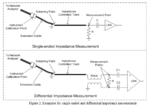
That is almost the same way I do in-board impedance/returnloss measurement. The only difference is that I still calibrate VNA at the SMA connector end using standard calibration kit. While I use the s1p files collected
from the three steps you describe above to do the calibration work myself. The advantage of my method lies that you can solder the extension cable to the board first, then do the calibration at the measurement point on PCB:
"OPEN": disconnect the connection at the measurement point;
"SHORT": short the measurement point to GND (of course the connection to the circuit is still cut-off);
"MATCH": solder 50 or 75 Ohm resistor to GND (as you said, use two or more resistors in parallel could reduce the parasite inductance);
"LOAD": connect to the circuit input or output.

Then the cable soldering point could be far away from the measurement pad as long as there is connection between those two points. This usually makes the soldering work much easier.
 

A method I generally use for this is including a small through line in a test PCB for my circuit and registering it as "through" is calibration; hence it is engraved into the calibration.

That cable you showed: It's name as far as I know is "pig-tail" connector; however they tend to get worse with each soldering. A similar approach can be installing UFL connectors in your PCB for test connections.

You can also use 2 seperate calibration kits; one of them N-type other is SMA-type, to include effect of adapters and fixture loss in your measurements.
 
That is almost the same way I do in-board impedance/returnloss measurement. The only difference is that I still calibrate VNA at the SMA connector end using standard calibration kit. While I use the s1p files collected
from the three steps you describe above to do the calibration work myself. The advantage of my method lies that you can solder the extension cable to the board first, then do the calibration at the measurement point on PCB:
"OPEN": disconnect the connection at the measurement point;
"SHORT": short the measurement point to GND (of course the connection to the circuit is still cut-off);
"MATCH": solder 50 or 75 Ohm resistor to GND (as you said, use two or more resistors in parallel could reduce the parasite inductance);
"LOAD": connect to the circuit input or output.

Then the cable soldering point could be far away from the measurement pad as long as there is connection between those two points. This usually makes the soldering work much easier.
Here is a picture of my method. A picture is worthy 1000 words.
impedance_measurement.PNG

- - - Updated - - -

A method I generally use for this is including a small through line in a test PCB for my circuit and registering it as "through" is calibration; hence it is engraved into the calibration.

That cable you showed: It's name as far as I know is "pig-tail" connector; however they tend to get worse with each soldering. A similar approach can be installing UFL connectors in your PCB for test connections.

You can also use 2 seperate calibration kits; one of them N-type other is SMA-type, to include effect of adapters and fixture loss in your measurements.

Agree the thin extension cable tend to get worn out very quickly. The insulation gets melt during soldering. I have to cut-off the head and make a new soldering tip from time to time. Then the cable becomes shorter and shorter...:cry:
 
  • Like
Reactions: ktr

    ktr

    Points: 2
    Helpful Answer Positive Rating
I recommend you to use 2 identical semi-rigid cables, connected back-to-back on a single independent pad while sharing the GND in very short distance in order to do a consistent calibration.
 

Status
Not open for further replies.

Part and Inventory Search

Welcome to EDABoard.com

Sponsor

Back
Top