Continue to Site

Welcome to EDAboard.com

Welcome to our site! EDAboard.com is an international Electronics Discussion Forum focused on EDA software, circuits, schematics, books, theory, papers, asic, pld, 8051, DSP, Network, RF, Analog Design, PCB, Service Manuals... and a whole lot more! To participate you need to register. Registration is free. Click here to register now.

[SOLVED] FPGA coding style behavioral vs structural modeling

Status
Not open for further replies.

eengr

Member level 4
Member level 4
Joined
Mar 9, 2016
Messages
75
Helped
0
Reputation
0
Reaction score
0
Trophy points
1,286
Activity points
4,270
FPGA coding style Behavioural vs structural Modelling

Hi All
I would like to use Xilinx Spartan-6 XC6SLX9 (TQFP-144) to design an address decoder for ISA Bus. The board would be connected to PC104 and will use ISA bus 8-bit data line to communicate. The task is to:

  1. Direct the data from ISA 8-bit data-lines to 1st set of 8-bit OUTPUT lines of FPGA if address on ISA Address bus is say 0x500.
  2. Direct the data from ISA 8-bit data-lines to 2nd set of 8-bit OUTPUT lines of FPGA if address on ISA Address bus is say 0x502.
  3. Direct the data from 1st set of 8-bit INPUT lines from FPGA to 8 bit ISA Data bus if the address on ISA Address bus is say 0x503.
  4. Direct the data from 2nd set of 8-bit INPUT lines from FPGA to 8 bit ISA Data bus if the address on ISA Address bus is say 0x504.


Off course ISA bus has its IOR & IOW lines that could be read to find out if it is Read operation or Write operation. Also, the clock signal is coming from ISA bus (PC104)

I am new to FPGA design & VHDL. This design has been done in the past by someone using schematic entry on Xilinx ISE using a different Xilinx FPGA device (which has gone obsolete) but I would like to use VHDL for it.

I have seen VHDL generated file of the old design and it looks more like component and instantiation in I think what is known as "Structural Modelling Style" (port mapping is generated for all logical symbols used in schematic entry)

If I look at the task at hand, it looks "simple" to me in that, I think could be implemented by using simple 'if' statements for above 4 cases & many be use CLK signal in process sensitivity list. I understand that it is something called 'Behavioural Modelling Style' i.e., looking at the inputs & outputs only (and treating everything in the middle as black box)

But then I started looking into a book 'Digital System Design with VHDL' by Mark Zwolinski in order to dig bit deeper to find out if 'Behavioural Style' would be a reasonable approach for me to take
I have attached the two pages of his book Page42.jpgPage41.jpg with this message
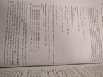
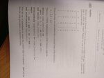
On page -42 it states that: While this model is perfectly acceptable as a description of a particular logical function, it does not correspond to any normally available piece of circuitry

Now, I am confused and struggling to understand if using Behavioural Modelling style will be good enough for my design OR would I need to start looking into Structural Modelling style? And what are the pros & cons (for this specific case) OR have i got wrong end of stick?
Any help would be greatly appreciated..
 

Re: FPGA coding style Behavioural vs structural Modelling

I think there is a big misunderstanding as to what "behavioural style" and "structural style" really mean.
"Structural style" should really mean instantiating base level primitives and wiring them together. This is just a netlist, and may prevent synthesisor optimizations.
"Behavioral style" (otherwise known as RTL) is writing code that will infer low level primitives from more abstracted code. This is basically what HDLs were designed to do.

People can get confused when they write some lower level functions in behavioral style then instantiate a ton of them and wire them together.

In reality, only masochists and "oldschool" engineers really use true "structural style" code. Behavioural style (RTL) is what everyone usually uses.
The Schematics editors are essentially structural style code shown graphically. Schematics have mostly fallen out of favor for engineers for many reasons (not portable, dont play well with versions control, cant simulate etc etc).

If you are a beginner, "structural style" can help you map your understanding directly from gates to code. Other than that, it gets really bloated, hard to understand and engineers really dont like it.

Hi TrickyDicky

Thank you very much for the reply and explanation. So, am I correct in saying that by using any one of these methods Behavioural (that I would prefer as it seems far easier to implement when I look at the task from Top level - Dare I say more like C-Code) or Structural (Effectively getting down to gate levels and netlist - making it cumbersome - Dare I say more like Assembly language), I should be able to achieve same result for the task that I am working at? OR is there something inherently different between the two approaches that would favour Structural over Behavioural?
 

Re: FPGA coding style Behavioural vs structural Modelling

#3,

I'm going to throw a spanner in the works.

behavioural is often a term used for testbench code which may be non-synthesisble.

RTL is the term you want to be using which implies synthesisible code.

An example of structural, rtl and beh is give below


Code VHDL - [expand]
1
2
3
4
5
6
7
8
9
10
11
12
13
14
15
16
17
18
19
20
21
22
23
24
25
26
27
28
29
30
31
32
33
34
architecture struct of my_entity is
 
fd : fdre
port map(r, clk, d, q, qn)
 
...
 
architecture rtl of my_entity is
 
process(clk) is
constant not_active : std_logic := '0';
begin
  if r then
    q <= not_active;
    qn <= not not_active;
  elsif rising_edge(clk) then
    q <= d;
    qn <= not d;
  end if;
end process;
 
...
 
architecture beh of my_entity is
 
process 
begin
  q <= not_active; qn <= not not_active;
  wait until r = '0'; 
  loop
    wait until rising_edge(clk);
    q <= d;
    exit when r = '1';
  end loop;


You'll find that you us structural to describe your block diagrams, rtl to implement your functionality and beh to test your functionality.

You mention structural for primatives and gates, whereas structural can be a much high level of abstraction for representation of entities and modules linked together (block diagrams).

Regarding favouring one or the other.... If you have the functionality of an entity or primitive or whatever you want to call it then you can instantiate that in structural level, you may need to add some additional control if the blocks dont' interface perfectly (thereby making a hybrid architecture). If you haven't got the functionality yet then you program it using rtl or beh.
 
  • Like
Reactions: eengr

    eengr

    Points: 2
    Helpful Answer Positive Rating
Re: FPGA coding style Behavioural vs structural Modelling

Writing register assignments in a non-synthesizable style like your "beh" code isn't a good example if you want to show that behavioral is different from RTL, I think. I would look at behavioral code that doesn't directly translate to RTL, e.g. using variables or loops and other more abstract constructs. It can still be synthesizable and a useful method of hardware design entry. Like Tricky, I would subsume it under RTL in my code, although it's probably a bit beyond.

VHDL for simulation can of course do anything.
 
  • Like
Reactions: eengr

    eengr

    Points: 2
    Helpful Answer Positive Rating
Re: FPGA coding style Behavioural vs structural Modelling

Hi there

Thanks for the feedback. OK I will use the correct terminology as RTL vs structural.

For this task, if I use the code similar to following:


Code VHDL - [expand]
1
2
3
4
5
6
7
8
9
10
11
12
13
14
15
16
17
18
19
20
21
22
23
24
25
26
27
28
29
30
31
32
33
34
35
36
37
38
39
40
41
42
43
44
45
46
47
[CODE]library IEEE;
use IEEE.STD_LOGIC_1164.ALL;
 
-- Uncomment the following library declaration if using
-- arithmetic functions with Signed or Unsigned values
--use IEEE.NUMERIC_STD.ALL;
 
-- Uncomment the following library declaration if instantiating
-- any Xilinx primitives in this code.
--library UNISIM;
--use UNISIM.VComponents.all;
 
entity myboard is
    Port (  ISA_ABUS_IN : in  STD_LOGIC_VECTOR (19 downto 0);
            ISA_DBUS_INOUT : inout  STD_LOGIC_VECTOR (7 downto 0);
            ISA_IOR : in  STD_LOGIC;
            ISA_IOW : in  STD_LOGIC;
            ISA_CLK: in STD_LOGIC;  -- ISA_OSC is clock signal coming from ISA BUS PC104 side
            FPGA_DBUS_OUT1: out STD_LOGIC_VECTOR (7 downto 0);
            FPGA_DBUS_OUT2: out STD_LOGIC_VECTOR (7 downto 0);
            FPGA_DBUS_OUT3: out STD_LOGIC_VECTOR (7 downto 0);
            FPGA_DBUS_OUT4: out STD_LOGIC_VECTOR (7 downto 0);
            FPGA_OSC : in  STD_LOGIC ); -- FPGA_OSC is 50MHz oscilltor on myboard (not used in the code below)
              
end myboard;
 
architecture Behavioral of myboard is
 
begin
                process (ISA_CLK, ISA_IOR,ISA_IOW)
                begin
                    if (ISA_IOR = '0' or ISA_IOW = '0') then
                        if (ISA_CLK'event and ISA_CLK = '1') then
                                if (ISA_ABUS_IN = "00000000010100000000") then -- if address is 0x500
                                    FPGA_DBUS_OUT1 <= ISA_DBUS_INOUT;
                                elsif (ISA_ABUS_IN = "00000000010100000001") then -- if address is 0x501
                                    FPGA_DBUS_OUT2 <= ISA_DBUS_INOUT;
                                elsif (ISA_ABUS_IN = "00000000010100000010" then -- if address is 0x502
                                    ISA_DBUS_INOUT <= FPGA_DBUS_OUT3;
                                elsif (ISA_ABUS_IN = "00000000010100000011" then -- if address is 0x503
                                    ISA_DBUS_INOUT <= FPGA_DBUS_OUT4;
                                                                
                                end if;
                        end if;
                end process;
 
end Behavioral;[/CODE]


instead of using the structural code, that basically represents the netlist and use port mapping of each individual block in schematic (in order to achieve the same results at Outputs / IOs as above), then would the two styles work in same way? As the above code is only few lines and is relatively simpler/easier to enter as compared to hundreds of lines of structural code that was generated as a result of schematic level entry....
 
Last edited:

Re: FPGA coding style Behavioural vs structural Modelling

would the two styles work in same way?
Functional equivalent code can be expected to result in the same gate level implementation.

I guess that the latest code is meant as a simplified example, it does actually not implement the read operation correctly, particularly misses to tristate the data bus. You need to check carefully if the bus driver enable is required to act synchronous or asynchronously and implement the intended operation strictly in RTL code.
 
  • Like
Reactions: eengr

    eengr

    Points: 2
    Helpful Answer Positive Rating
Re: FPGA coding style Behavioural vs structural Modelling

Hi there

OK, thanks for the clarification. I have implemented the changes and I believe that following code should work:


Code VHDL - [expand]
1
2
3
4
5
6
7
8
9
10
11
12
13
14
15
16
17
18
19
20
21
22
23
24
25
26
27
28
29
30
31
32
33
34
35
36
37
38
39
40
41
42
43
44
45
46
47
48
49
50
51
52
53
54
55
56
57
58
59
60
61
62
63
64
65
66
67
68
69
70
71
72
73
74
75
76
77
78
79
80
81
82
83
84
85
86
87
88
89
90
91
92
93
94
95
96
97
98
99
100
101
102
103
104
105
106
107
108
109
110
111
112
113
114
115
116
117
118
119
120
121
122
123
124
125
126
127
128
129
130
131
132
133
134
135
136
137
138
139
140
141
142
143
144
145
146
147
148
149
150
151
152
153
154
155
156
157
158
159
160
161
162
163
164
165
166
167
168
169
170
[CODE] library IEEE;
 
use IEEE.STD_LOGIC_1164.ALL;
use IEEE.STD_LOGIC_ARITH.ALL;
use IEEE.STD_LOGIC_UNSIGNED.ALL;


-- Uncomment the following library declaration if using
 
-- arithmetic functions with Signed or Unsigned values
 
--use IEEE.NUMERIC_STD.ALL;


-- Uncomment the following library declaration if instantiating
 
-- any Xilinx primitives in this code.
 
--library UNISIM;
 
--use UNISIM.VComponents.all;


entity P0344ISAvhd is
 
    Port (  ISA_ABUS_IN : in  STD_LOGIC_VECTOR (19 downto 0);
 
            ISA_DBUS_INOUT : inout  STD_LOGIC_VECTOR (7 downto 0);
 
            ISA_IOR : in  STD_LOGIC;
 
            ISA_IOW : in  STD_LOGIC;
 
            ISA_IO16 : out STD_LOGIC;
 
            ISA_DATA_EN : out STD_LOGIC; --  Enable line for Level Shifter IC on Data Bus
 
            ISA_DATA_DIR: out STD_LOGIC; -- Direction line for Level Shifter IC on Data Bus
 
            ISA_CLK: in STD_LOGIC;  -- ISA_OSC is clock signal coming from ISA BUS PC104 side
 
            FPGA_DBUS_INOUT1: inout STD_LOGIC_VECTOR (7 downto 0);
 
            FPGA_DBUS_INOUT2: inout STD_LOGIC_VECTOR (7 downto 0);
 
            FPGA_DBUS_IN1: in   STD_LOGIC_VECTOR (7 downto 0));
 
        --  FPGA_DBUS_IN2: in   STD_LOGIC_VECTOR (7 downto 0));
 
          --  FPGA_OSC : in  STD_LOGIC ); -- FPGA_OSC is 50MHz oscilltor on myboard (not used in the code below)


end P0344ISAvhd;


architecture Behavioral of P0344ISAvhd is
 
signal ISA_DBUS : STD_LOGIC_VECTOR (7 downto 0) := (others => '0');
signal FPGA_DBUS1 : STD_LOGIC_VECTOR (7 downto 0) := (others => '0');
signal FPGA_DBUS2 : STD_LOGIC_VECTOR (7 downto 0) := (others => '0');


begin
 
                process (ISA_CLK, ISA_IOR,ISA_IOW)


                begin
 
                    if (ISA_CLK'event and ISA_CLK = '1') then
 
                        if (ISA_IOW = '0' and ISA_IOR = '1') then -- Write is enabled
 
                            ISA_IO16 <= '0'; -- It is NOT an 16 bit device
 
                            ISA_DATA_DIR <= '0'; -- Set Direction of Data Bus Level TxRx as ISA to FPGA
 
                            ISA_DATA_EN <= '0'; -- Enable the Data Bus Level TxRx
 
                            if (ISA_ABUS_IN = "00000000010100000000") then -- if address is 0x500
 
                                FPGA_DBUS1 <= ISA_DBUS;
 
                                ISA_DBUS_INOUT <= ISA_DBUS;
 
                                FPGA_DBUS_INOUT1 <= FPGA_DBUS1;
 
                            elsif (ISA_ABUS_IN = "00000000010100000001") then -- if address is 0x501
 
                                FPGA_DBUS2 <= ISA_DBUS;
 
                                ISA_DBUS_INOUT <= ISA_DBUS;
 
                                FPGA_DBUS_INOUT2 <= FPGA_DBUS2;
 
                            end if;
                        --ISA_DBUS_INOUT <= ISA_DBUS;
 
                        --FPGA_DBUS_INOUT1 <= FPGA_DBUS1;
                        --FPGA_DBUS_INOUT2 <= FPGA_DBUS2;
 
                        ISA_DATA_EN <= '1'; -- Disable the Data Bus Level TxRx  
 
                        end if;


                        if (ISA_IOW = '1' and ISA_IOR = '0') then -- Read is enabled
 
                            ISA_IO16 <= '0'; -- It is NOT an 16 bit device
 
                            ISA_DATA_DIR <= '1'; -- Set Direction of Data Bus Level TxRx as FPGA to ISA
 
                            ISA_DATA_EN <= '0'; -- Enable the Data Bus Level TxRx
 
                            if (ISA_ABUS_IN = "00000000010100000000") then -- if address is 0x500
 
                                ISA_DBUS <= FPGA_DBUS1;
 
                                ISA_DBUS_INOUT <= ISA_DBUS;
 
                                FPGA_DBUS_INOUT1 <= FPGA_DBUS1;
 
                            elsif (ISA_ABUS_IN = "00000000010100000001") then -- if address is 0x501
 
                                ISA_DBUS <= FPGA_DBUS2;
 
                                ISA_DBUS_INOUT <= ISA_DBUS;
 
                                FPGA_DBUS_INOUT2 <= FPGA_DBUS2;
 
                            elsif (ISA_ABUS_IN = "00000000010100000010") then -- if address is 0x502
 
                                ISA_DBUS <= FPGA_DBUS_IN1;
 
                                ISA_DBUS_INOUT <= ISA_DBUS;
 
                        --  elsif (ISA_ABUS_IN = "00000000010100000011") then -- if address is 0x503
 
                            --  ISA_DBUS <= FPGA_DBUS_IN2;
 
                            --  ISA_DBUS_INOUT <= ISA_DBUS;


                            end if;
                        --ISA_DBUS_INOUT <= ISA_DBUS;
 
                        --FPGA_DBUS_INOUT1 <= FPGA_DBUS1;
                        --FPGA_DBUS_INOUT2 <= FPGA_DBUS2;
 
                        ISA_DATA_EN <= '1'; -- Disable the Data Bus Level TxRx
 
                        end if;
                    end if;
 
                end process;


end Behavioral; [/CODE]


I am using it for only three cases when Address on Address Bus is 0x500, 0x501 & 0x502 (4th case is commented out)


But when I tried to run the Behavioural Simulation, (setting address to 0x500 first & then 0x501 --- putting Data on ISA_DBUS_INOUT as "01100101" first & then "01011001" (see my test bench code below)

Code VHDL - [expand]
1
2
3
4
5
6
7
8
9
10
11
12
13
14
15
16
17
18
19
20
21
22
23
24
25
26
27
28
29
30
31
32
33
34
35
36
37
38
39
40
41
42
43
44
45
46
47
48
49
50
51
52
53
54
55
56
57
58
59
60
61
62
63
64
65
66
67
68
69
70
71
72
73
74
75
76
77
78
79
80
81
82
83
84
85
86
87
88
89
90
91
92
93
94
95
96
97
98
99
100
101
102
103
104
105
106
107
108
109
110
111
112
113
114
115
116
117
118
119
120
121
122
123
124
125
--------------------------------------------------------------------------------
-- Company: 
-- Engineer:
--
-- Create Date:   13:56:50 10/31/2018
-- Design Name:   
-- Module Name:   /home/ise/Shared_Folder/Fpga_Vhd/P0344ISAvhd/P0344ISA_TB.vhd
-- Project Name:  P0344ISAvhd
-- Target Device:  
-- Tool versions:  
-- Description:   
-- 
-- VHDL Test Bench Created by ISE for module: P0344ISAvhd
-- 
-- Dependencies:
-- 
-- Revision:
-- Revision 0.01 - File Created
-- Additional Comments:
--
-- Notes: 
-- This testbench has been automatically generated using types std_logic and
-- std_logic_vector for the ports of the unit under test.  Xilinx recommends
-- that these types always be used for the top-level I/O of a design in order
-- to guarantee that the testbench will bind correctly to the post-implementation 
-- simulation model.
--------------------------------------------------------------------------------
LIBRARY ieee;
USE ieee.std_logic_1164.ALL;
 
-- Uncomment the following library declaration if using
-- arithmetic functions with Signed or Unsigned values
--USE ieee.numeric_std.ALL;
 
ENTITY P0344ISA_TB IS
END P0344ISA_TB;
 
ARCHITECTURE behavior OF P0344ISA_TB IS 
 
    -- Component Declaration for the Unit Under Test (UUT)
 
    COMPONENT P0344ISAvhd
    PORT(
         ISA_ABUS_IN : IN  std_logic_vector(19 downto 0);
         ISA_DBUS_INOUT : INOUT  std_logic_vector(7 downto 0);
         ISA_IOR : IN  std_logic;
         ISA_IOW : IN  std_logic;
         ISA_IO16 : OUT  std_logic;
         ISA_DATA_EN : OUT  std_logic;
         ISA_DATA_DIR : OUT  std_logic;
         ISA_CLK : IN  std_logic;
         FPGA_DBUS_INOUT1 : INOUT  std_logic_vector(7 downto 0);
         FPGA_DBUS_INOUT2 : INOUT  std_logic_vector(7 downto 0);
         FPGA_DBUS_IN1 : IN  std_logic_vector(7 downto 0)
        );
    END COMPONENT;
    
 
   --Inputs
   signal ISA_ABUS_IN : std_logic_vector(19 downto 0) := (others => '0');
   signal ISA_IOR : std_logic := '0';
   signal ISA_IOW : std_logic := '0';
   signal ISA_CLK : std_logic := '0';
   signal FPGA_DBUS_IN1 : std_logic_vector(7 downto 0) := (others => '0');
 
    --BiDirs
   signal ISA_DBUS_INOUT : std_logic_vector(7 downto 0);
   signal FPGA_DBUS_INOUT1 : std_logic_vector(7 downto 0);
   signal FPGA_DBUS_INOUT2 : std_logic_vector(7 downto 0);
 
    --Outputs
   signal ISA_IO16 : std_logic;
   signal ISA_DATA_EN : std_logic;
   signal ISA_DATA_DIR : std_logic;
 
   -- Clock period definitions
   constant ISA_CLK_period : time := 125 ns; -- For 8MHz ISA Clock
 
BEGIN
 
    -- Instantiate the Unit Under Test (UUT)
   uut: P0344ISAvhd PORT MAP (
          ISA_ABUS_IN => ISA_ABUS_IN,
          ISA_DBUS_INOUT => ISA_DBUS_INOUT,
          ISA_IOR => ISA_IOR,
          ISA_IOW => ISA_IOW,
          ISA_IO16 => ISA_IO16,
          ISA_DATA_EN => ISA_DATA_EN,
          ISA_DATA_DIR => ISA_DATA_DIR,
          ISA_CLK => ISA_CLK,
          FPGA_DBUS_INOUT1 => FPGA_DBUS_INOUT1,
          FPGA_DBUS_INOUT2 => FPGA_DBUS_INOUT2,
          FPGA_DBUS_IN1 => FPGA_DBUS_IN1
        );
 
   -- Clock process definitions
   ISA_CLK_process :process
   begin
        ISA_CLK <= '0';
        wait for ISA_CLK_period/2;
        ISA_CLK <= '1';
        wait for ISA_CLK_period/2;
   end process;
 
 
   -- Stimulus process
   stim_proc: process
   begin        
      -- hold reset state for 100 ns.
      wait for 100 ns;  
 
      wait for ISA_CLK_period*10;
        
      -- insert stimulus here 
        ISA_IOW <= '0';
        ISA_IOR <= '1';
        ISA_ABUS_IN <= "00000000010100000000";
        ISA_DBUS_INOUT <= "01100101";
        wait for ISA_CLK_period*2;
        ISA_ABUS_IN <= "00000000010100000001";
        ISA_DBUS_INOUT <= "01011001";
      wait;
   end process;
 
END;


I ran the simulation for 2000ns, it showed change of address on ISA_ABUS_IN as 00000000010100000000 & then 00000000010100000001
It also shows changes on ISA_DBUS_INOUT from 0XX00X0X & then 0X0XX00X

But Data on ISA_DBUS_INOUT stayed as all Zeroes throughout

However, the data on
FPGA_DBUS_INOUT1
&
FPGA_DBUS_INOUT2

always stays at 00000000

Please see my behavioral simulation waveform below:

Behavioural Simulation_original.png

I am not sure what and where I am wrong here... Any help would be greatly appreciated.

PS: If this question is deviating from my original post & title of the post then please let me know & I will start a new Post for this..
 
Last edited by a moderator:

Re: FPGA coding style Behavioural vs structural Modelling

Don't use both code and syntax tags together (I fixed it and left only the syntax tags).

You have inout on the ISA_DBUS_INOUT, but your testbench always drives it to a value, so the X's appear due to driving some bits to opposite logic levels in your testbench and in your DUT. You also have no logic to high-Z the bus in the DUT, so there is no way the bus can even be used as an INOUT it is code as an OUT only.

- - - Updated - - -

Other notable things:
Code:
                process (ISA_CLK, ISA_IOR,ISA_IOW)
                begin
                    if (ISA_CLK'event and ISA_CLK = '1') then
                        if (ISA_IOW = '0' and ISA_IOR = '1') then -- Write is enabled
process sensitivity list has extra signals. Only ISA_CLK is required, the other two are not required as the process is NOT sensitive to them, they are synchronous inputs that are only looked at when the clock occurs.

use the function rising_edge(ISA_CLK) instead of ISA_CLK'event and ISA_CLK = '1' as the function will correctly deal with things like U/Z/X to 1 transitions, whereas the 'event will consider all transitions from anything other than 1 valid clock transitions.

Also you can use x"0500" instead of the unreadable "0000010100000000" if your simulator isn't something ancient.

- - - Updated - - -

However, the data on
FPGA_DBUS_INOUT1
&
FPGA_DBUS_INOUT2

always stays at 00000000


It stays all zeros because you assign it all 0's and never assign anything else to it.
Code:
signal FPGA_DBUS_IN1 : std_logic_vector(7 downto 0) := (others => '0');
FPGA_DBUS_IN1 => FPGA_DBUS_IN1
if (ISA_ABUS_IN = "00000000010100000000") then -- if address is 0x500
    FPGA_DBUS_INOUT1 <= FPGA_DBUS1;
See it's assigned 0's in the signal declaration and just gets propagated to the INOUT port.

As VHDL is a hardware description language, maybe it would help if you drew a schematic of what you are trying to design and then describe that design in VHDL. Right now I get the impression that you are "hacking" the code together without seeing the hardware logic you require.
 
  • Like
Reactions: eengr

    eengr

    Points: 2
    Helpful Answer Positive Rating
Re: FPGA coding style Behavioural vs structural Modelling

Although your on the way to write behavioral code, it could help to sketch the planned register and tri-state driver topology, also symbolize the test bench by hardware elements.
 
  • Like
Reactions: eengr

    eengr

    Points: 2
    Helpful Answer Positive Rating
Re: FPGA coding style Behavioural vs structural Modelling

Don't use both code and syntax tags together (I fixed it and left only the syntax tags).

Thanks for correction, I will keep that in mind next time :)


As VHDL is a hardware description language, maybe it would help if you drew a schematic of what you are trying to design and then describe that design in VHDL. Right now I get the impression that you are "hacking" the code together without seeing the hardware logic you require.

I have a rough schematic as below:
Schematic.png

Please ignore the crossed areas as I am not using (well I am hoping that I have not used them) them in my VHDL code

I am sure I have made number of mistakes in my code (few of them have already been highlighted in last message) but it would be good to know if I am on right path now or do I need something different here !?! I think in addition to test bench code, I am struggling to implement INOUT function of port correctly in my DUT particularly when I want to read the status of an Output port (FPGA_DBUS_INOUT1 )for instance
 

Re: FPGA coding style Behavioural vs structural Modelling

That schematic from the original (?) design is helpful as it shows some of the stuff you are missing in your HDL, namely:
Capture.PNG
No where do you have that tri-state driver in your code.

You need something like this:

Code VHDL - [expand]
1
fpga_dbus_inouta <= dbus1 when en = '1' else (others => 'Z');

 
  • Like
Reactions: eengr

    eengr

    Points: 2
    Helpful Answer Positive Rating
Re: FPGA coding style Behavioural vs structural Modelling

That schematic from the original (?) design

Yes, the design was originally done using schematic entry for an older version of FPGA that has gone obsolete now. & I would like to use VHDL (and trying to avoid using/modifying the VHDL file generated from original design as it is effectively a long structural modelling (netlist of various blocks used) & to make things worse I am newbie to VHDL/FPGA world
is helpful as it shows some of the stuff you are missing in your HDL, namely:
View attachment 149785
No where do you have that tri-state driver in your code.

You need something like this:

Code VHDL - [expand]
1
fpga_dbus_inouta <= dbus1 when en = '1' else (others => 'Z');


Where would I need to declare this tristate in my code? As it has EN line so do I need to first create an entity of Buffer with Enable and use port mapping (Separate component declaration & instantiation) OR could I use the IOW OR IOR line as EN for the above

& I am struggling to figure out a way to read the status of output ports (FPGA_DBUS_INOUT1) in VHDL
 

Re: FPGA coding style Behavioural vs structural Modelling

The line of code I posted is how you would generate the FPGA_DBUS_INOUT1 port on your DUT.
You will assign EN with whatever logic was connected to that AND gate.

Forget about instantiating a tri-state driver in your code. Stop fixating on structural vs behavioral code.

Just write the code using code that describes what you are trying to accomplish. e.g. the tri-state code in my previous post describes that the output FPGA_DBUS_INOUT is driven by an internal signal DBUS1 when it is enabled with EN being 1 otherwise it is hi-Z. That describes the function instead of instantiating a tri-state.

In some rare cases you have to instantiate (structural code) to implement features in the FPGA you are using as there is no way to write behavioral code the synthesis tool can infer the required logic (e.g. DDR input registers usually fall under this category)

In summary

Code VHDL - [expand]
1
2
3
4
5
6
7
8
9
10
11
12
13
port (
    INOUT_PORT    : inout std_logic
);
 
signal temp1 : std_logic;
signal temp2 : std_logic;
signal en : std_logic;
 
-- used as an input
temp1 <= INOUT_PORT;
 
-- driven as an output
INOUT_PORT <= temp2 when en = '1' else 'Z';

 
  • Like
Reactions: eengr

    eengr

    Points: 2
    Helpful Answer Positive Rating
Re: FPGA coding style Behavioural vs structural Modelling

thanks for the reply.

I have modified my code now as:


Code VHDL - [expand]
1
2
3
4
5
6
7
8
9
10
11
12
13
14
15
16
17
18
19
20
21
22
23
24
25
26
27
28
29
30
31
32
33
34
35
36
37
38
39
40
41
42
43
44
45
46
47
48
49
50
51
52
53
54
55
56
57
58
59
60
61
62
63
64
65
66
67
68
69
70
71
72
73
74
75
76
77
78
79
80
81
82
83
84
85
86
87
88
89
90
91
92
93
94
95
96
97
98
99
100
101
102
103
104
105
106
107
108
109
110
111
112
113
114
115
116
117
118
119
120
121
122
123
124
125
126
127
128
129
130
131
132
133
134
135
136
137
138
139
140
141
142
143
144
145
146
147
148
149
150
151
152
153
154
155
156
library IEEE;
 
use IEEE.STD_LOGIC_1164.ALL;
use IEEE.STD_LOGIC_ARITH.ALL;
use IEEE.STD_LOGIC_UNSIGNED.ALL;


-- Uncomment the following library declaration if using
 
-- arithmetic functions with Signed or Unsigned values
 
--use IEEE.NUMERIC_STD.ALL;


-- Uncomment the following library declaration if instantiating
 
-- any Xilinx primitives in this code.
 
--library UNISIM;
 
--use UNISIM.VComponents.all;


entity P0344ISAvhd is
 
    Port (  ISA_ABUS_IN : in  STD_LOGIC_VECTOR (19 downto 0);
 
            ISA_DBUS_INOUT : inout  STD_LOGIC_VECTOR (7 downto 0);
 
            ISA_IOR : in  STD_LOGIC;
 
            ISA_IOW : in  STD_LOGIC;
 
            ISA_IO16 : out STD_LOGIC;
 
            ISA_DATA_EN : out STD_LOGIC; --  Enable line for Level Shifter IC on Data Bus
 
            ISA_DATA_DIR: out STD_LOGIC; -- Direction line for Level Shifter IC on Data Bus
 
            ISA_CLK: in STD_LOGIC;  -- ISA_OSC is clock signal coming from ISA BUS PC104 side
 
            FPGA_DBUS_OUT1: out STD_LOGIC_VECTOR (7 downto 0);
 
            FPGA_DBUS_OUT2: out STD_LOGIC_VECTOR (7 downto 0);
 
            FPGA_DBUS_IN1: in   STD_LOGIC_VECTOR (7 downto 0));
 
        --  FPGA_DBUS_IN2: in   STD_LOGIC_VECTOR (7 downto 0));
 
          --  FPGA_OSC : in  STD_LOGIC ); -- FPGA_OSC is 50MHz oscilltor on myboard (not used in the code below)


end P0344ISAvhd;


architecture Behavioral of P0344ISAvhd is
 
signal ISA_DBUS1 : STD_LOGIC_VECTOR (7 downto 0) := (others => '0');
signal ISA_DBUS2 : STD_LOGIC_VECTOR (7 downto 0) := (others => '0');
signal FPGA_DBUS11 : STD_LOGIC_VECTOR (7 downto 0) := (others => '0');
--signal FPGA_DBUS12 : STD_LOGIC_VECTOR (7 downto 0) := (others => '0');
signal FPGA_DBUS21 : STD_LOGIC_VECTOR (7 downto 0) := (others => '0');
--signal FPGA_DBUS22 : STD_LOGIC_VECTOR (7 downto 0) := (others => '0');
signal en1 : STD_LOGIC;


begin
                ISA_DBUS1 <= ISA_DBUS_INOUT; -- Used as an input
                ISA_DBUS_INOUT <= ISA_DBUS2 when en1 = '1' else "ZZZZZZZZ"; -- Used as an output
 
                FPGA_DBUS_OUT1 <= FPGA_DBUS11; -- Signal assigned to output
                
                FPGA_DBUS_OUT2 <= FPGA_DBUS21; -- Signal assigned to output
                
 
                process (ISA_CLK)


                begin


                    if (rising_edge (ISA_CLK)) then
 
                        if (ISA_IOW = '0' and ISA_IOR = '1') then -- Write is enabled
                            en1 <= '0';
                            ISA_IO16 <= '0'; -- It is NOT an 16 bit device
 
                            ISA_DATA_DIR <= '0'; -- Set Direction of Data Bus Level TxRx as ISA to FPGA
 
                            ISA_DATA_EN <= '0'; -- Enable the Data Bus Level TxRx
 
                            if (ISA_ABUS_IN = X"0500") then -- if address is 0x500
                                FPGA_DBUS11 <= ISA_DBUS1;
 
                            elsif (ISA_ABUS_IN = X"0501") then -- if address is 0x501
                                FPGA_DBUS21 <= ISA_DBUS1;
                                                        
 
                            end if;


                        end if;


                        if (ISA_IOW = '1' and ISA_IOR = '0') then -- Read is enabled
                            en1 <= '1';
 
                            ISA_IO16 <= '0'; -- It is NOT an 16 bit device
 
                            ISA_DATA_DIR <= '1'; -- Set Direction of Data Bus Level TxRx as FPGA to ISA
 
                            ISA_DATA_EN <= '0'; -- Enable the Data Bus Level TxRx
 
                            if (ISA_ABUS_IN = X"0500") then -- if address is 0x500
                                ISA_DBUS2 <= FPGA_DBUS11;
 
                            elsif (ISA_ABUS_IN = X"0501") then -- if address is 0x501
                                ISA_DBUS2 <= FPGA_DBUS21;
                                
 
                            elsif (ISA_ABUS_IN = X"0502") then -- if address is 0x502
                                ISA_DBUS2 <= FPGA_DBUS_IN1;


                            end if;


                        end if;
                        
                        if (ISA_IOW = '1' and ISA_IOR = '1') then -- Read is enabled
                            ISA_DATA_EN <= '1';
                        end if;
                    end if;
 
                end process;


end Behavioral;


I think I need INOUT (bidirectional) Port at ISA_DBUS_INOUT only. And the other two ports FPGA_DBUS_OUT1 & FPGA_DBUS_OUT2 would be used as Output ports only for actual application. However, we would need to read the status of these Output ports which believe is done by using Signals rather than declaring these as INOUT ports

I think that above code should work but then it does not work when I try it in simulation as it looks like when the ISA_DBUS_INOUT is used as OUTPUT, there is a clash.
My Test bench code is:


Code VHDL - [expand]
1
2
3
4
5
6
7
8
9
10
11
12
13
14
15
16
17
18
19
20
21
22
23
24
25
26
27
28
29
30
31
32
33
34
35
36
37
38
39
40
41
42
43
44
45
46
47
48
49
50
51
52
53
54
55
56
57
58
59
60
61
62
63
64
65
66
67
68
69
70
71
72
73
74
75
76
77
78
79
80
81
82
83
84
85
86
87
88
89
90
91
92
93
94
95
96
97
98
99
100
101
102
103
104
105
106
107
108
109
110
111
112
113
114
115
116
117
118
119
120
121
122
123
124
125
126
127
128
129
130
131
132
133
134
--------------------------------------------------------------------------------
-- Company: 
-- Engineer:
--
-- Create Date:   15:31:08 11/01/2018
-- Design Name:   
-- Module Name:   /home/ise/Shared_Folder/Fpga_Vhd/P0344ISAvhd/P0344ISA_TB5.vhd
-- Project Name:  P0344ISAvhd
-- Target Device:  
-- Tool versions:  
-- Description:   
-- 
-- VHDL Test Bench Created by ISE for module: P0344ISAvhd
-- 
-- Dependencies:
-- 
-- Revision:
-- Revision 0.01 - File Created
-- Additional Comments:
--
-- Notes: 
-- This testbench has been automatically generated using types std_logic and
-- std_logic_vector for the ports of the unit under test.  Xilinx recommends
-- that these types always be used for the top-level I/O of a design in order
-- to guarantee that the testbench will bind correctly to the post-implementation 
-- simulation model.
--------------------------------------------------------------------------------
LIBRARY ieee;
USE ieee.std_logic_1164.ALL;
 
-- Uncomment the following library declaration if using
-- arithmetic functions with Signed or Unsigned values
--USE ieee.numeric_std.ALL;
 
ENTITY P0344ISA_TB5 IS
END P0344ISA_TB5;
 
ARCHITECTURE behavior OF P0344ISA_TB5 IS 
 
    -- Component Declaration for the Unit Under Test (UUT)
 
    COMPONENT P0344ISAvhd
    PORT(
         ISA_ABUS_IN : IN  std_logic_vector(19 downto 0);
         ISA_DBUS_INOUT : INOUT  std_logic_vector(7 downto 0);
         ISA_IOR : IN  std_logic;
         ISA_IOW : IN  std_logic;
         ISA_IO16 : OUT  std_logic;
         ISA_DATA_EN : OUT  std_logic;
         ISA_DATA_DIR : OUT  std_logic;
         ISA_CLK : IN  std_logic;
         FPGA_DBUS_OUT1 : OUT  std_logic_vector(7 downto 0);
         FPGA_DBUS_OUT2 : OUT  std_logic_vector(7 downto 0);
         FPGA_DBUS_IN1 : IN  std_logic_vector(7 downto 0)
        );
    END COMPONENT;
    
 
   --Inputs
   signal ISA_ABUS_IN : std_logic_vector(19 downto 0) := (others => '0');
   signal ISA_IOR : std_logic := '0';
   signal ISA_IOW : std_logic := '0';
   signal ISA_CLK : std_logic := '0';
   signal FPGA_DBUS_IN1 : std_logic_vector(7 downto 0) := (others => '0');
 
    --BiDirs
   signal ISA_DBUS_INOUT : std_logic_vector(7 downto 0);
 
    --Outputs
   signal ISA_IO16 : std_logic;
   signal ISA_DATA_EN : std_logic;
   signal ISA_DATA_DIR : std_logic;
   signal FPGA_DBUS_OUT1 : std_logic_vector(7 downto 0);
   signal FPGA_DBUS_OUT2 : std_logic_vector(7 downto 0);
 
   -- Clock period definitions
   constant ISA_CLK_period : time := 125 ns; --8MHz clock for ISA Bus
 
BEGIN
 
    -- Instantiate the Unit Under Test (UUT)
   uut: P0344ISAvhd PORT MAP (
          ISA_ABUS_IN => ISA_ABUS_IN,
          ISA_DBUS_INOUT => ISA_DBUS_INOUT,
          ISA_IOR => ISA_IOR,
          ISA_IOW => ISA_IOW,
          ISA_IO16 => ISA_IO16,
          ISA_DATA_EN => ISA_DATA_EN,
          ISA_DATA_DIR => ISA_DATA_DIR,
          ISA_CLK => ISA_CLK,
          FPGA_DBUS_OUT1 => FPGA_DBUS_OUT1,
          FPGA_DBUS_OUT2 => FPGA_DBUS_OUT2,
          FPGA_DBUS_IN1 => FPGA_DBUS_IN1
        );
 
   -- Clock process definitions
   ISA_CLK_process :process
   begin
        ISA_CLK <= '0';
        wait for ISA_CLK_period/2;
        ISA_CLK <= '1';
        wait for ISA_CLK_period/2;
   end process;
 
 
   -- Stimulus process
   stim_proc: process
   begin        
      -- hold reset state for 100 ns.
      wait for 100 ns;  
 
      wait for ISA_CLK_period*10;
        ISA_IOW <= '0';
        ISA_IOR <= '1';
        ISA_ABUS_IN <= "00000000010100000000";
        ISA_DBUS_INOUT <= "01100101";
        wait for ISA_CLK_period*2;
        ISA_ABUS_IN <= "00000000010100000001";
        ISA_DBUS_INOUT <= "01011001";
        wait for ISA_CLK_period*2;
        ISA_IOW <= '1';
        ISA_IOR <= '0';
        ISA_ABUS_IN <= "00000000010100000000";
        wait for ISA_CLK_period*2;
        ISA_ABUS_IN <= "00000000010100000001";


      -- insert stimulus here 
 
      wait;
   end process;
 
END;


& My wave forms are:

Behavioural Simulation_clash.png

What am I doing wrong now?
 

Re: FPGA coding style Behavioural vs structural Modelling

The problem has been already addressed, e.g. by ads-ee in post #9. You need to tristate the bus in the test bench when performing a read.


Code VHDL - [expand]
1
2
ISA_IOR <= '0';
 ISA_DBUS_INOUT <= "ZZZZ;


However, we would need to read the status of these Output ports.
What do you mean by status of the output ports? You can easily read back the content of the output registers.
 
  • Like
Reactions: eengr

    eengr

    Points: 2
    Helpful Answer Positive Rating
Re: FPGA coding style Behavioural vs structural Modelling

However, we would need to read the status of these Output ports which believe is done by using Signals rather than declaring these as INOUT ports
Older vs newer versions of the VHDL standard...

Old VHDL: OUT ports cannot be read by logic that is internal to the architecture.
New VHDL: OUT port read restrictions were relaxed to allow reading output ports in the architecture.

Just make an internal version of the output port and use that everywhere in your code, then assign that internal signal to the OUT port. Now you can continue to compile your code using the older VHDL standard. Other option is to set your compilation/synthesis to VHDL2005+
 
  • Like
Reactions: eengr

    eengr

    Points: 2
    Helpful Answer Positive Rating
Re: FPGA coding style Behavioural vs structural Modelling

Thanks for the feedback I Modifed Stimulus as:


Code VHDL - [expand]
1
2
3
4
5
6
7
8
9
10
11
12
13
14
15
16
17
18
19
20
21
22
23
24
25
26
27
28
stim_proc: process
   begin        
      -- hold reset state for 100 ns.
      wait for 100 ns;  
 
      wait for ISA_CLK_period*10;
        FPGA_DBUS_IN1 <= "01010101";
        ISA_IOW <= '0';
        ISA_IOR <= '1';
        ISA_ABUS_IN <= "00000000010100000000";
        ISA_DBUS_INOUT <= "01100101";
        wait for ISA_CLK_period*2;
        ISA_ABUS_IN <= "00000000010100000001";
        ISA_DBUS_INOUT <= "01011001";
        wait for ISA_CLK_period*2;
        ISA_IOW <= '1';
        ISA_IOR <= '0';
        ISA_DBUS_INOUT<="ZZZZZZZZ";
        ISA_ABUS_IN <= "00000000010100000000";
        wait for ISA_CLK_period*2;
        ISA_ABUS_IN <= "00000000010100000001";
        wait for ISA_CLK_period*2;
        ISA_ABUS_IN <= "00000000010100000010";
 
      -- insert stimulus here 
 
      wait;
   end process;


& obtained Waveforms as:
Behavioural Simulation_ZZ.png


These are much better results but would like to improve my test bench so that 'ZZ' is not shown in the waveforms (if possible). Also, if I try another write cycle after the Read (toggling IOW to '0') i.e.,


Code VHDL - [expand]
1
2
3
4
5
6
7
8
9
10
11
12
13
14
15
16
17
18
19
20
21
22
23
24
25
26
27
28
29
30
31
stim_proc: process
   begin        
      -- hold reset state for 100 ns.
      wait for 100 ns;  
 
      wait for ISA_CLK_period*10;
        FPGA_DBUS_IN1 <= "01010101";
        ISA_IOW <= '0';
        ISA_IOR <= '1';
        ISA_ABUS_IN <= "00000000010100000000";
        ISA_DBUS_INOUT <= "01100101";
        wait for ISA_CLK_period*2;
        ISA_ABUS_IN <= "00000000010100000001";
        ISA_DBUS_INOUT <= "01011001";
        wait for ISA_CLK_period*2;
        ISA_IOW <= '1';
        ISA_IOR <= '0';
        ISA_DBUS_INOUT<="ZZZZZZZZ";
        ISA_ABUS_IN <= "00000000010100000000";
        wait for ISA_CLK_period*2;
        ISA_ABUS_IN <= "00000000010100000001";
        wait for ISA_CLK_period*2;
        ISA_ABUS_IN <= "00000000010100000010";
                wait for ISA_CLK_period*2;
                ISA_ABUS_IN <= "00000000010100000001";
        ISA_DBUS_INOUT <= "11111001"
 
      -- insert stimulus here 
 
      wait;
   end process;


then the waveforms show clash as I think ISA_DBUS_INOUT is still in ZZZZZZZZ

I tried the following


Code VHDL - [expand]
1
2
3
4
5
6
7
8
9
10
11
12
13
14
15
16
17
18
19
20
21
22
23
24
25
26
27
28
29
30
31
32
33
34
35
36
37
38
39
40
41
42
43
44
45
46
47
48
49
50
51
52
53
54
55
56
57
58
59
60
61
62
63
64
65
66
67
68
69
70
71
72
73
74
75
76
77
78
79
80
81
82
83
84
85
86
87
88
89
90
91
92
93
94
95
96
97
98
99
100
101
102
103
104
105
106
107
108
109
110
111
112
113
114
115
116
117
118
119
120
121
122
--------------------------------------------------------------------------------
 
LIBRARY ieee;
USE ieee.std_logic_1164.ALL;
 
-- Uncomment the following library declaration if using
-- arithmetic functions with Signed or Unsigned values
--USE ieee.numeric_std.ALL;
 
ENTITY P0344ISA_TB5 IS
END P0344ISA_TB5;
 
ARCHITECTURE behavior OF P0344ISA_TB5 IS 
 
    -- Component Declaration for the Unit Under Test (UUT)
 
    COMPONENT P0344ISAvhd
    PORT(
         ISA_ABUS_IN : IN  std_logic_vector(19 downto 0);
         ISA_DBUS_INOUT : INOUT  std_logic_vector(7 downto 0);
         ISA_IOR : IN  std_logic;
         ISA_IOW : IN  std_logic;
         ISA_IO16 : OUT  std_logic;
         ISA_DATA_EN : OUT  std_logic;
         ISA_DATA_DIR : OUT  std_logic;
         ISA_CLK : IN  std_logic;
         FPGA_DBUS_OUT1 : OUT  std_logic_vector(7 downto 0);
         FPGA_DBUS_OUT2 : OUT  std_logic_vector(7 downto 0);
         FPGA_DBUS_IN1 : IN  std_logic_vector(7 downto 0)
        );
    END COMPONENT;
    
 
   --Inputs
   signal ISA_ABUS_IN : std_logic_vector(19 downto 0) := (others => '0');
   signal ISA_IOR : std_logic := '0';
   signal ISA_IOW : std_logic := '0';
   signal ISA_CLK : std_logic := '0';
   signal FPGA_DBUS_IN1 : std_logic_vector(7 downto 0) := (others => '0');
 
    --BiDirs
   signal ISA_DBUS_INOUT : std_logic_vector(7 downto 0);
 
    --Outputs
   signal ISA_IO16 : std_logic;
   signal ISA_DATA_EN : std_logic;
   signal ISA_DATA_DIR : std_logic;
   signal FPGA_DBUS_OUT1 : std_logic_vector(7 downto 0);
   signal FPGA_DBUS_OUT2 : std_logic_vector(7 downto 0);
 
   -- Clock period definitions
   constant ISA_CLK_period : time := 125 ns; --8MHz clock for ISA Bus
    signal TEMP_DBUS_INOUT : std_logic_vector(7 downto 0);
BEGIN
    
    
    -- Instantiate the Unit Under Test (UUT)
   uut: P0344ISAvhd PORT MAP (
          ISA_ABUS_IN => ISA_ABUS_IN,
          ISA_DBUS_INOUT => ISA_DBUS_INOUT,
          ISA_IOR => ISA_IOR,
          ISA_IOW => ISA_IOW,
          ISA_IO16 => ISA_IO16,
          ISA_DATA_EN => ISA_DATA_EN,
          ISA_DATA_DIR => ISA_DATA_DIR,
          ISA_CLK => ISA_CLK,
          FPGA_DBUS_OUT1 => FPGA_DBUS_OUT1,
          FPGA_DBUS_OUT2 => FPGA_DBUS_OUT2,
          FPGA_DBUS_IN1 => FPGA_DBUS_IN1
        );
        ISA_DBUS_INOUT <= TEMP_DBUS_INOUT when ISA_IOR = '1' else "ZZZZZZZZ"; -- Used as an output
   -- Clock process definitions
   ISA_CLK_process :process
   begin
        ISA_CLK <= '0';
        wait for ISA_CLK_period/2;
        ISA_CLK <= '1';
        wait for ISA_CLK_period/2;
   end process;
 
 
   -- Stimulus process
   stim_proc: process
   begin        
      -- hold reset state for 100 ns.
        
        
      wait for 100 ns;  
 
      wait for ISA_CLK_period*10;
        FPGA_DBUS_IN1 <= "01010101";
        ISA_IOW <= '0';
        ISA_IOR <= '1';
        ISA_ABUS_IN <= "00000000010100000000";
        TEMP_DBUS_INOUT <= "01100101";
        wait for ISA_CLK_period*2;
        ISA_ABUS_IN <= "00000000010100000001";
        TEMP_DBUS_INOUT <= "01011001";
        wait for ISA_CLK_period*2;
        ISA_ABUS_IN <= "00000000010100000010"; -- Check the effect of this case during Write cycle
        wait for ISA_CLK_period*2;
        ISA_IOW <= '1';
        ISA_IOR <= '0';
        --ISA_DBUS_INOUT<="ZZZZZZZZ";
        ISA_ABUS_IN <= "00000000010100000000";
        wait for ISA_CLK_period*2;
        ISA_ABUS_IN <= "00000000010100000001";
        wait for ISA_CLK_period*2;
        ISA_ABUS_IN <= "00000000010100000010";
        wait for ISA_CLK_period*2;
        ISA_IOW <= '0';
        ISA_IOR <= '1';
        ISA_ABUS_IN <= "00000000010100000000";
        TEMP_DBUS_INOUT <= "11111101";
        wait for ISA_CLK_period*2;
 
      -- insert stimulus here 
 
      wait;
   end process;
 
END;


which basically adds


Code VHDL - [expand]
1
ISA_DBUS_INOUT <= TEMP_DBUS_INOUT when ISA_IOR = '1' else "ZZZZZZZZ"; -- Used as an output


Line to the testbench in hope that ISA_DBUS_INOUT would take value of TEMP_DBUS_INOUT or else appear as ZZZZZ

But it shows clashes on second Write cycle (See Red in waveforms below)

Behavioural Simulation_ZZ_Clash.png


What do I need to change in tb code?
 

Re: FPGA coding style Behavioural vs structural Modelling

The X's have nothing to do with your testbench, it looks like a problem with your DUT.

Given the code snippets from earlier, you probably have a clock cycle delay before the output from your DUT goes to an active value.
 
  • Like
Reactions: eengr

    eengr

    Points: 2
    Helpful Answer Positive Rating
Re: FPGA coding style Behavioural vs structural Modelling

The problem has been already addressed, e.g. by ads-ee in post #9. You need to tristate the bus in the test bench when performing a read.


Code VHDL - [expand]
1
2
ISA_IOR <= '0';
 ISA_DBUS_INOUT <= "ZZZZ;


Is there a way to get ISA_DBUS_INOUT out from High impedance mode (so that it behaves like Output) after it has been put into High Impedance mode once in Test Bench?
I know I did this in EUT as suggested by ads-ee & FvM but how do I implement it in testbench? I was think of testbench of more like a test setup that is used to test the EUT without actually manipulating the EUT, but it looks like we need to do some stuff with the ports of EUT as part of testing (that I was hoping, EUT should be able to pick up from its own code)

What do you mean by status of the output ports? You can easily read back the content of the output registers.

The way I understand is that I need to create internal signals in VHDL to read the output registers & that's how I did it in my code.

The X's have nothing to do with your testbench, it looks like a problem with your DUT.

Given the code snippets from earlier, you probably have a clock cycle delay before the output from your DUT goes to an active value.

I am struggling to find any delays in my DUT code as I haven't used any counter/timers for any delays in my code. I am using same DUT code as in my post #15
 

Status
Not open for further replies.

Part and Inventory Search

Welcome to EDABoard.com

Sponsor

Back
Top