Continue to Site

Welcome to EDAboard.com

Welcome to our site! EDAboard.com is an international Electronics Discussion Forum focused on EDA software, circuits, schematics, books, theory, papers, asic, pld, 8051, DSP, Network, RF, Analog Design, PCB, Service Manuals... and a whole lot more! To participate you need to register. Registration is free. Click here to register now.

Altium: unrouted net when using copper to connect

Status
Not open for further replies.

shootme

Newbie level 3
Newbie level 3
Joined
Jan 19, 2018
Messages
3
Helped
0
Reputation
0
Reaction score
0
Trophy points
1
Activity points
47
I'm having an issue with connection errors and I can't figure out how to get rid of them, as they don't seem to be real.
screen:
copper.png

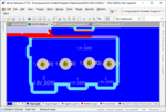
I have quite a few power pours that are running on internal layers. I'm using copper on the top to connect the net to caps, resistors, beads, etc, and dropping vias that connect that to the internal pour. Unfortunately, Altium is reporting un-routed nets anywhere that I'm using the copper as a means of connection.

"Un-Routed Net Constraint: Net 3.3V_DAC Between Pad C165-2(-3629mil,-2656.99mil) on Top Layer And Via (-3600mil,-2655mil) from Top Layer to Bottom Layer "

I've tried using solid regions and pours and both behaved the same.
The copper is associated with the proper net and I have "pour over same net objects" selected.
I looked into tweaking the un-routed net rules, but I didn't see a way to select multiple objects that wouldn't mask true errors.

I was just going to ignore these rules, but in the 230 reported, I've already found a few that are legitimate un-routed nets. My other obvious solution is to run traces within the copper between the components that are throwing the errors, but that will be rather tedious (and a bit of a waste of time).

Am I overlooking something? Is there something I can do in the design rules to ignore this while not masking real errors? I'm worried that I'm going to miss an actual unrouted net in this jumble.

thanks for the help
 

If you have already linked the copper plan to the desired net and are still not being routed, it may be that the PAD you drew above, for some mysterious reason, should not contain all the layers.
 

This seems to be happening everywhere that I'm using this technique, the screen shot is just one example.

It doesn't seem to be an issue with a single footprint, but I'll look closer.

The copper is assigned to the proper net and pour over same net objects is selected.

pour.png
 

I got frustrated with this again today and realized that the error ONLY shows up with vias. Mostly pad to via, sometimes via to via, but never pad to pad. Again, my problem with this is that I currently have 251 reported errors. Of these, only a handful are real and I found one today that was unintentional.

Here's an example of the errors I get for a given net:

Un-Routed Net Constraint: Net 1.8V_DDR2 Between Pad C167-2(-2643.188mil,-2595.001mil) on Top Layer And Via (-2627mil,-2616mil) from Top Layer to Bottom Layer
Un-Routed Net Constraint: Net 1.8V_DDR2 Between Via (-2627mil,-2616mil) from Top Layer to Bottom Layer And Pad C170-2(-2625mil,-2642.765mil) on Top Layer
Un-Routed Net Constraint: Net 1.8V_DDR2 Between Via (-2589.093mil,-2615.443mil) from Top Layer to Bottom Layer And Pad C170-2(-2625mil,-2642.765mil) on Top Layer
Un-Routed Net Constraint: Net 1.8V_DDR2 Between Pad C177-2(-2568.93mil,-2644mil) on Top Layer And Via (-2589.093mil,-2615.443mil) from Top Layer to Bottom Layer
Un-Routed Net Constraint: Net 1.8V_DDR2 Between Pad C182-2(-2521.92mil,-2643mil) on Top Layer And Via (-2516.013mil,-2615.443mil) from Top Layer to Bottom Layer
Un-Routed Net Constraint: Net 1.8V_DDR2 Between Pad FB14-1(-2558mil,-2586.38mil) on Top Layer And Via (-2549mil,-2614mil) from Top Layer to Bottom Layer
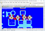
This is what the net looks like, with a poured over via
pourover.png

OUt of curiosity, I started looking at the via connect method for polygons. I largely use pour over for maximum current and heat transfer, but I changed to the default thermal connection, just to see what it looked like:
thermal.png

When I poured with the thermals, the vias show lack of connection, the same that are being reported when I use the pour-over method. I tried setting a design rule that doesn't check 'partial connections' when the object is a polygon (where object matches InPolygon), but nothing changed - I was hoping the arc approximation was leading to a partial connection at the via's center.

Has anyone experienced this and found a fix? Work around? Is it just a glitch in the program? Any ideas?

I'd hate to spin a board and have a blatant error that was missed because of this.

THanks
 

Shootme, did you ever figure anything out about this issue? I finished a board today and when I ran DRC I have 365 similar errors. All look to be perfect via in pours. I plan to check tomorrow it is all vias in pours, pads, blind/buried, or just all vias period. Very frustrating
 

IMG_20180419_074758.jpg

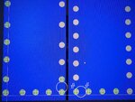
In the picture you can clearly see the vias are in the same pour but only some show an unrouted net constraint error. These vias were placed at the same time. They all connect to top, bottom, and internal power planes. I have other projects with the same rule set that do not have this issue. At a loss
 

Hi. I have the same problem today. Suggest a solution. You can remove vias and then add them again. This helpad me. If via will only touch the pad then there should be a track to solve this. If removing/adding will not help. Try to remove and then add vias but first via place in the center of pad and other around. Another solutions dont have)) Dont what is this - glitch or somthing else...

another problem is found. Sometimes all these solutions dont help. Then try to do the gap between vias more. I think this problem may appeat when two vias are very close to each other and touch each other and altium shows this like "incomplete connection" but with track this problem cant be solved. dont know why
 
Last edited:
You can remove vias and then add them again

You likely nailed it; really looks like the vias are not with the GND net associated with them, perhaps there is the standard "no net" connection there at the vias. Another possible solution is to double click at each via and manually assign a net, but a lot of work depending on how many are there.
 

No, vias are associated with gnd.
For this can be used inspector maybe.
In my case, where a lot of vias are almost touch each other can be simple removed tick "check for incomplete connection". but this isn't good solution.. straaange
 

Status
Not open for further replies.

Part and Inventory Search

Welcome to EDABoard.com

Sponsor

Back
Top