Continue to Site

Welcome to EDAboard.com

Welcome to our site! EDAboard.com is an international Electronics Discussion Forum focused on EDA software, circuits, schematics, books, theory, papers, asic, pld, 8051, DSP, Network, RF, Analog Design, PCB, Service Manuals... and a whole lot more! To participate you need to register. Registration is free. Click here to register now.

what design specifications are important in pcb manufacturing for LNA's?

Status
Not open for further replies.
Anyway, your "expert" on YT is stupidly wrong.

https://www.youtube.com/watch?v=SwNb0ndIT5k&t=354s

starting (2:25 - 2:42), they are Rogers Corp. ACS.

- - - Updated - - -

You forget working at 2.4GHz.Everything is critical at RF.
Typical GND connection of a stub or grounded components should be as follows.
View attachment 146339

is this better?

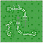
https://imgur.com/a/ayc7bf4

, some of the 0402 components I couldn't seem to get 5 vias surrounded, only 4.
 

The via design and CPW discussion is surely interesting, but - as I feel - related to the present design somehow missing the point.

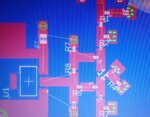
detail.jpg

I see e.g. this points
- it's not really relevant how much via inductance connects a 550 ohm resistor. A single via would be just fine.
- but you have an unconnected FET source pin, and more than necessary trace length at the other source pin's bypass capacitor.

Generally I'm curious how the LNA dimensioning has been derived.

The Eagle airlines would disappear if the traces are routing the connections correctly. Something is apparently wrong.
 
- but you have an unconnected FET source pin.

Generally I'm curious how the LNA dimensioning has been derived.

The Eagle airlines would disappear if the traces are routing the connections correctly. Something is apparently wrong.


I thought the unconnected source pin would be fine, because I am using the other source pin; aren't the two source pins connected internally?

I derived the dimensions by making sure that I had the components as close as possible, to an extent to keep the design less cumbersome to manufacture. I didn't want to put the components back to back, which may cause a difficult way to solder the components together. I also didn't want to create problems where I may not have enough room to pass a t-line around the transistor. I also saw other designs where the gate and drain t-lines would be oriented in a consistent line path; which is why the transistor is tilted at a 45 degree. I also kept the lines less than 1/10 of a wavelength at 2.4 GHz.

Just letting you know, I am a newbie at Eagle. I know for sure I organized the components correctly and I don't know why the air lines are still there. I thought the air lines were there to guide me where each component should be placed? I used the rect function to create rectangular transmission lines because I couldn't find a routing option that has rectangular strips. The only option to connect the components was to use routing with strips that have a semicircle at the end of the line (which I thought would effect Zo = 50 ohm). Further more, while I am using the routing option and I specified a width of the line that is larger than the width of the component, this would create an issue that would make the line cross over to the other terminal side, creating a short. This is why I wanted to customize my own t-line using rect function, so I have a specific width (to keep Zo = 50), a certain length (1/10 wavelength), and to keep the whole components terminal leads directly on the t-line without overpassing to the other side of the component.
 
Last edited:

I thought the unconnected source pin would be fine, because I am using the other source pin; aren't the two source pins connected internally?

Yes they are. However, two are brought out to lower the effective inductance. To get even close to your design requirements with this board, you're going to have to connect both sources to the proper termination.

To get rid of the airwires, you have to connect the center of the pad to the centerline of the trace. You can do this by placing a very thin line inside the dimensions of your microstrip line that connects the center of the pad to the centerline of the trace.
 
  • Like
Reactions: skatefast08

    V

    Points: 2
    Helpful Answer Positive Rating

    skatefast08

    Points: 2
    Helpful Answer Positive Rating
To get rid of the airwires, you have to connect the center of the pad to the centerline of the trace. You can do this by placing a very thin line inside the dimensions of your microstrip line that connects the center of the pad to the centerline of the trace.

would this do any significant change in the actual circuit?
 

would this do any significant change in the actual circuit?

If done correctly, it won't have any effect on the circuit. This is basically putting metal on metal (which in the end, is just metal). With small parts that have pad centers off the grid that you are using, this is the way it is done. To do this, click ROUTE and at the pad, start laying down a trace, staying inside the boundaries of your µstrip line. You can then terminate the route by connecting the end to the centerline of the bigger line. It might look ugly on the screen, but once fabricated, you'll never know that it ever happened.
 
  • Like
Reactions: skatefast08

    V

    Points: 2
    Helpful Answer Positive Rating

    skatefast08

    Points: 2
    Helpful Answer Positive Rating
To get even close to your design requirements with this board, you're going to have to connect both sources to the proper termination.

does the size of the strip matter (will it effect the characteristic impedance) when connecting the unconnected source pin to the other source pin? if I used a smaller strip to connect, would you think it would significantly change the performance of the LNA?

- - - Updated - - -

You forget working at 2.4GHz.Everything is critical at RF.
Typical GND connection of a stub or grounded components should be as follows.
View attachment 146339

Does the orientation or the separation of the vias have any significant impact? since you said the vias should be close to the associated component, I have recognized that when you put the vias in a semi circular pattern rather than in a rectangular fashion (as you did) around the pin of the component, the vias can more close-packed on the component terminal. Would this be a better approach, since they become more closely packed? should I give a certain distance between the vias? also, would it be better if the vias are actually touching the terminal?
 

does the size of the strip matter (will it effect the characteristic impedance) when connecting the unconnected source pin to the other source pin? if I used a smaller strip to connect, would you think it would significantly change the performance of the LNA?

The bigger, the better. You don't have to run square ends to your devices. You can safely neck them down, as shown below.

route.jpg

Here is a µwave mixer board laid out in CPW. The entire bottom is a solid ground plane, except where the SMAs poke thru:

Mixer.jpg
 
Last edited:

    V

    Points: 2
    Helpful Answer Positive Rating
what would you use for a power plug-in device for the LNA using a 9v battery? would you solder the 9v battery snap-connector wires to the board, or would you let the manufacture do that?
 

If it's battery powered, you don't need (or want) the regulator in your circuit (they add to the noise). But to answer your question, have your builder add the 9V battery clip to the board, with leads long enough to reach the battery compartment.
 

Good advice SLK001. A note to skatefast08, GCP has the via fence along the trace. The via spacing "must be" less than 1/4 wavelength of your highest operating frequency. Vias are cheep... keeping in mind the you need a capture pad for the vias.
I often use a "linear" regulator on LNAs. Switching regulators is very bad for LNAs.
 

I have a specific width (to keep Zo = 50), a certain length (1/10 wavelength)

You misunderstood the rule. The rule is for the line between 50 ohm circuit parts. You have have a lumped circuits with many SMD, that's a different topic than connecting 50 Ohm circuit blocks. For your case, the rule is: Keep all the lines as short as possible, with parasitics from layout (series L or shunt C) as small as possible.
 

You misunderstood the rule. The rule is for the line between 50 ohm circuit parts. You have have a lumped circuits with many SMD, that's a different topic than connecting 50 Ohm circuit blocks.

Would it be more efficient and convenient to use 50 ohm blocks or to put the components as compact as possible? How would you know if the component are 50 ohm? does the component have to be the same size as the line?
 
Last edited:

An example for a 50 ohm block is an entire amplifier specified for 50 Ohm operation, or a mixer or filter with 50 ohm/in out. Single elements inside the circuit usually are not 50 ohm blocks.

For your LNA that was simulated without transmission line effects, make lines as short as possible. Try to be as close as possible to the lumped (zero size) circuit that you designed.

The usual RF design method is to include lines in simulation, then you see what you get.
 
Last edited:

-Silkscreen and solder-maks is not necessary.But immersion gold plating may improve the performance.

I left out silkscreen and soldermask for the manufacture, do you think this is a good idea? I asked one of the customer service PCB ladies at the company she first says these are included into the circuit without an additional fee. She gives me a hard time by asking me, "if without solder mask to be made, how do you do the assembly?" then she also says, "yes, you need to have the solder mask opening to solder the components."

I also ask if she can leave out silkscreen too, then she says, "but usually silkscreen is needed for assembly, so we can know where to solder the components."

all of this makes me a bit confused and unsure if this will effect my LNA if I do not include these features. She is a bit convincing that I should include these properties. Please, should I leave out soldermask and silkscreen? or should it be included?

I did include the immersion gold though for the surface finish. Is HASL not as effective or something?
 
Last edited:

I left out silkscreen and soldermask for the manufacture, do you think this is a good idea?

Yes, leave out, it's not needed. Anything that is placed over the traces can effect the operation of the circuit. Generally, engineers don't take advice from assembly line personnel.

I did include the immersion gold though for the surface finish. Is HASL not as effective or something?

For a µwave PCB, the gold is better than most other finishes. HASL is not as well controlled as the gold.

I also ask if she can leave out silkscreen too, then she says, "but usually silkscreen is needed for assembly, so we can know where to solder the components."

She's wrong. Silkscreen is not needed for assembly, either by hand, or automatic.
 
how bout solderpaste?

With a proper solder stencil, solder paste is just fine.

I'm assuming that you are using pick-and-place machines to populate your board and then a reflow oven in air to complete the soldering. Even without soldermask, your results will be just fine.
 

Status
Not open for further replies.

Similar threads

Part and Inventory Search

Welcome to EDABoard.com

Sponsor

Back
Top