Continue to Site

Welcome to EDAboard.com

Welcome to our site! EDAboard.com is an international Electronics Discussion Forum focused on EDA software, circuits, schematics, books, theory, papers, asic, pld, 8051, DSP, Network, RF, Analog Design, PCB, Service Manuals... and a whole lot more! To participate you need to register. Registration is free. Click here to register now.

What will be the logic ckt?

Status
Not open for further replies.

samiran_dam

Full Member level 2
Full Member level 2
Joined
Apr 17, 2010
Messages
122
Helped
3
Reputation
6
Reaction score
3
Trophy points
1,298
Activity points
2,419
Hi All,

I have to generate an o/p from two i/p signals (A & B) as shown in the following fig. What kind of logic ckt. should I to achieve this?

Drawing1.jpg
 

I don't find any straight forward combinational circuit that can help you achieve this sort of output from signals A and B.

But you can try some sequential circuit in which the output depends on the current inputs as well as previous state of inputs.
 

You want the output to be high from the falling edge of 'A' until the falling edge of 'B'. You should be able to use a flip-flop or S-R latch to do that.

Brian.
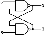
 

You want the output to be high from the falling edge of 'A' until the falling edge of 'B'. You should be able to use a flip-flop or S-R latch to do that.

Brian.
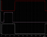
Yes, I also attempted to achieve this using a NAND based latch. However, not able to generate the desired o/p signal. Not quite sure how to do that. Any help is appreciated. I guess, a simple latch will not help the cause; it may require a edge-triggered SR flip-flop, but I am not getting any suitable edge-triggered FF circuit.

34-sr-latch-nand.png
Capture.PNG
 

Hi,

do you need real hardware or code (HDL)?

****
Your diagram is not clear.
* what happens to the opitput when B is HIGH during the falling edge of A?
* what happens to the opitput when A is LOW during the falling edge of B?

Klaus
 

I need a real hardware, not a code!
So basically, the requirement is - o/p will be toggled to HIGH @negedge of i/p A and toggled to LOW @negedge of i/p B, o/p will not change its state @posedge of either A or B.
 
Hi,

o/p will not change its state @posedge of either A or B.
This is doesn´t answer my questions.

Klaus
 

Hi,

do you need real hardware or code (HDL)?

****
Your diagram is not clear.
* what happens to the opitput when B is HIGH during the falling edge of A?
* what happens to the opitput when A is LOW during the falling edge of B?

Klaus

* what happens to the opitput when B is HIGH during the falling edge of A?
This situation never occurs.
* what happens to the opitput when A is LOW during the falling edge of B?
this situation is already shown in the illustration given below.
Drawing1.jpg

So basically, let me explain one more time - the output should go to HIGH at the falling edge of 'A' and toggle to LOW at the next falling edge of 'B'.
 

Can you try a separate clock signal to provide edge triggering to run this logic ckt.
 

Hi,

* what happens to the opitput when A is LOW during the falling edge of B?
this situation is already shown in the illustration given below.
Yes, sorry. I meant:
* what happens to the opitput when A is HIGH during the falling edge of B?

Do you have a high speed clock source?
What are the timing specifications:
* A_falling to output
* A LOW time
* A HIGH time
* B_falling to output
* B LOW time
* B HIGH time
* All A to B timings

You may use a PLD and a (high speed) clock.
The smallest - maybe one IC solution - could be a 8 pin microcontroller.
...it depends on your timing specifications.

Klaus
 

Please provide an unequivocal function specification. The timing diagram in post #1 is useless because it doesn't show the state before and after the last input signal transition.
 

Please provide an unequivocal function specification. The timing diagram in post #1 is useless because it doesn't show the state before and after the last input signal transition.

But the waveform they used to simulate with in post #4 seems to indicate that the default state of A is high, the default state of B is low and the output should go high on falling edge of A and low on the falling edge of B.

I've been on the fence about answering this question. Not entirely sure if this is a homework problem or a real world problem they are trying to solve.
If it is homework, it's unfair to the rest of the students if you get your answer from a career engineer.
If it is your job, I have an issue with someone being hired to do a job they are not qualified to perform.

Because I like puzzles, I actually played around with this for 10 minutes yesterday and came up with two similar solutions.
  • One that requires a reset signal.
  • One that can self initialize but depending on the A and B initial state (a non-default state of A=1,B=0) it may have erroneous outputs until the first pulse occurs from then on it will be the correct output.

It might not be the best or most optimal solution, but I didn't spend a lot of time thinking about the problem. I'll give you a hint on what I did.
I used two falling edge D flip-flops and an XOR gate. Hmm actually that pretty much gives it away.
 

Status
Not open for further replies.

Part and Inventory Search

Welcome to EDABoard.com

Sponsor

Back
Top