Continue to Site

Welcome to EDAboard.com

Welcome to our site! EDAboard.com is an international Electronics Discussion Forum focused on EDA software, circuits, schematics, books, theory, papers, asic, pld, 8051, DSP, Network, RF, Analog Design, PCB, Service Manuals... and a whole lot more! To participate you need to register. Registration is free. Click here to register now.

Calibre LVS errors help

Status
Not open for further replies.

tenso

Advanced Member level 4
Full Member level 1
Joined
Feb 18, 2015
Messages
110
Helped
3
Reputation
6
Reaction score
2
Trophy points
1,298
Activity points
2,400
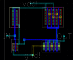
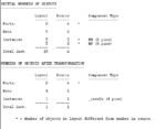
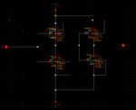
I am using calibre's LVS utility for the first time and I am getting some errors. I was trying to follow the PDK design flow document with a TSMC kit. I am attaching a screenshot of the layout (which was generated through Cadence's Chip Assembly Router), the schematic with which it is being compared to and the LVS report from calibre. The circuit itself is a 2 stage buffer.
LVS report.PNG

schematic.PNG

Layout.PNG

Apparently there are no ports in the layout even though I have included the labels for the IN, OUT, VDD and GND pins. Also both the multifinger transistors are showing up as 4 transistors, so my instance numbers are also different.
 

Looks like you have no substrate or well ties in your layout
 

Looks like you have no substrate or well ties in your layout


hey thanks for the reply. it seems you might be right. I have to at least connect the nwells to metal 1 here and metal 1 gnd to the p sub. I am using tsmc 180 and the layer pallet selection it doesn't appear that I have a via options M1 to NWELL and M1 to sub. Does anyone know if the NWELL pin and PWELL pin will be sufficient in this case?
 

hey thanks for the reply. it seems you might be right. I have to at least connect the nwells to metal 1 here and metal 1 gnd to the p sub. I am using tsmc 180 and the layer pallet selection it doesn't appear that I have a via options M1 to NWELL and M1 to sub. Does anyone know if the NWELL pin and PWELL pin will be sufficient in this case?

I can place a piece of an active (diffusion) inside Nwell covered by NPLUS, and piece of active/diffusion in SUB (covered by PPLUS).
Connect these diffusions to M1 by CONTACTs.
These will form (through LVS / extraction) a well tie.
 

I can place a piece of an active (diffusion) inside Nwell covered by NPLUS, and piece of active/diffusion in SUB (covered by PPLUS).
Connect these diffusions to M1 by CONTACTs.
These will form (through LVS / extraction) a well tie.

Hey thanks I for the reply. I fixed the nets issue by finding the M1_NWELL contact and a M1_PSUB contact. I didn't find the NPLUS and PPLUS connections you speak of though from the LSW. I have the following N_WELL and P_WELL contact instances in my library.

M1_NWELL
M1_NWELL_new
M1_NWELLc
M1_NWELLP

the same corresponding types are found for the PWELL contacts. Does anyone know what the difference between the last two is?

The only errors I have now in my LVS file is the number is instances and ports. How can force calibre to recognize parallel multifingered MOSFET devices as one?

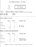
The following is the new report. As you can see I have fixed the nets issue with the well and substrate contacts as suggested.

Capture.PNG
 

Do you have your pins on the proper layers? Are you DRC clean?
 

Do you have your pins on the proper layers? Are you DRC clean?

I am getting about 12 or so errors during DRC and all of them appear to be dealing with minimum area and density requirements. Both power pins and input/output pins are using the metal 1 layer.
 

    borabilgic

    Points: 2
    Helpful Answer Positive Rating
I suspect there are metal_1 dwg (drawing) and metal_1 pin layers.
 

- - - Updated - - -

I suspect there are metal_1 dwg (drawing) and metal_1 pin layers.

you are right. I have been using metal 1 pin layers. should I have been using the drawing layers instead?
 

I have been using metal 1 pin layers. should I have been using the drawing layers instead?

No, the pin layer actually is correct for the pin names.

There must be a different reason for the LVS ports error.
Perhaps the pin layers hadn't been included for the extraction? Can you select the pins in the extracted view?
 

No, the pin layer actually is correct for the pin names.

There must be a different reason for the LVS ports error.
Perhaps the pin layers hadn't been included for the extraction? Can you select the pins in the extracted view?


I haven't extracted the cell yet so I don't have an extracted view created yet. Actually that was one of my other questions, we previously used DIVA from cadence for lvs purposes during coursework. DIVA only seems to compare the schematic with the extracted view.

All the examples of Calibre LVS I have seen so far seem to compare the layout (before extraction) with the schematic view.
 

DIVA only seems to compare the schematic with the extracted view.
Yes, that's correct. Same with ASSURA LVS.

All the examples of Calibre LVS I have seen so far seem to compare the layout (before extraction) with the schematic view.
I've no experience with Calibre LVS, so I can't help, sorry. But I think extraction is necessary in any case - how would you get a layout netlist (for comparison) by other means? I guess Calibre runs extraction in background anyway.

This doesn't necessarily mean parasitics extraction - just the layout connectivity to create a netlist.
 

I think some LVS errors generated due to not using M_CAD for text and you are using a different layer for text
This will be easier to be known if you tried to layout a signle NMOS and put all the pins required and do LVS for this single transsitor then do the same for a signle PMOS. Just to to make sure that you know how to connect the device pins and text and it can pass LVS.
Also sometimes the LVS error can raise an error flag if the centre of the text is not in the center of the pin (The LVS will not be sure that the text is not related to the specified Pin -- dumb errors but they happen)
 
Last edited:

Try looking in your extract rules and see if they tell specifically which layer spins must be on.

Try different combinations layers for your pins and make sure connectivity is on the pin. Place a text label on metal1_pin. Try it on metal1_drw.

Just some ideas.
 

Try looking in your extract rules and see if they tell specifically which layer spins must be on.

Try different combinations layers for your pins and make sure connectivity is on the pin. Place a text label on metal1_pin. Try it on metal1_drw.

Just some ideas.

so I was just looking up how to create pins from labels just to make sure I didn't mess anything up during the process. Turns out the text for the labels was a different layer than the pins themselves which were metal 1 layer. This document online has additional information. I think user MahmoudHassan above pointed this out.

**broken link removed**

I was generating the layout, pins and the connectivity from the source schematic as detailed above in Layout XL. Even though I chose metal 1 pin for the ports, I didn't change the layer for the text to "same as pin" option.

Anyway everyone thanks for the replies and trying to solve my issue. Now to figure out parasitic extraction using Calibre PEX.

Note: also before I forget, you don't need to parasitic extraction for running LVS in calibre. This is unlike cadence's DIVA and Assura (erikl said that ASSURA works the same as DIVA in this regard) Extraction doesn't seem to be separate step and is done by the LVS tool.

MODS can mark this as solved
 
Last edited:
  • Like
Reactions: erikl

    erikl

    Points: 2
    Helpful Answer Positive Rating
Note: also before I forget, you don't need to parasitic extraction for running LVS in calibre. This is unlike cadence's DIVA and Assura (erikl said that ASSURA works the same as DIVA in this regard) Extraction doesn't seem to be separate step and is done by the LVS tool.

Extraction for LVS and a parasitic extraction are two different things. Assura is run directly in Cadence. It may appear that an extraction is not being performed but it actually is. You have an extract rule set that creates a netlist of the layout. You will also have a compare ruleset that compares the extracted netlist vs the schematic netlist.

Calibre works the same but on a stream file and not DFII data.

Rulesets for parasitic extractions are written to extract parasitic devices (Rs, Cs & Ds) from a layout. I believe some tools can back annotate those devices into your schematic netlist.

thanks for trying to help earlier. yeah, I am aware that extraction for LVS is different from doing PEX. I was just saying that in DIVA you have to compare the PEX layout with your schematic. One of the mods said that ASSURA runs the same way. I was just pointing out that in Calibre LVS you don't need to PEX before hand.
 

Status
Not open for further replies.

Part and Inventory Search

Welcome to EDABoard.com

Sponsor

Back
Top